Paper Sharing
【Member Papers】A Novel 2.7 kV 3C-SiC/Ga₂O₃ Hetero-Channel E-mode MISFET With BFOM up to 5.17 GW/cm²
日期:2025-11-10阅读:452
Researchers from the University of Electronic Science and Technology of China have published a dissertation titled "A Novel 2.7 kV 3C-SiC/Ga2O3 Hetero-Channel E-mode MISFET With BFOM up to 5.17 GW/cm2" in Microelectronics Journal.
Background
β-Ga2O3 represents the most stable crystalline form of gallium oxide and is considered as a promising material for next-generation power devices due to its ultra-wide bandgap of 4.4-4.9 eV, high critical breakdown electric field (∼ 8 MV/cm). Despite these favorable characteristics, the absence of efficient p-type dopants in Ga2O3 remains a critical obstacle for high-voltage enhancement-mode (E-mode) metal-insulator-semiconductor field-effect transistors (MISFET). Several researches have been explored to fabricate E-mode high-voltage vertical MISFET, like current apertures and trench structures with high-resistivity layers, such as nitrogen-implantation or magnesium doped. However, the high-resistivity region causes unacceptable leakage current and increased specific on-resistance (Ron,sp). Fin-gate MISFET (FG-MISFET) has shown promising capabilities in achieving E-mode operation, reduced leakage current and high BV (The highest BV reaches 2.66 kV [10]). Another obstacle of MISFET is lack of an efficient electric field shielding structure, which causes pre-breakdown and reliability issues in the gate oxide. Similar to SiC MOSFET, the critical electric field (EC) in the gate oxide of Ga2O3 MISFET should be restricted to less than one-third of its theoretical value, which is approximately 5.3 MV/cm for Al2O3.
Abstract
In this letter, a novel 3C-SiC/Ga2O3 Hetero-Channel Ga2O3 MISFET (3C-HC-MISFET) for enhancement-mode (E-mode) operation, low specific on-resistance (Ron,sp) and low reverse on-state voltage drop (VR_ON) is proposed and demonstrated by experimentally calibrated TCAD. A p-type 3C-SiC layer is directly bonded atop β-Ga2O3 to form the inversion channel for E-mode operation. A heavily doped p-NiO layer under the trench gate suppresses the electric field in the gate dielectric. Besides, the p-NiO/Ga2O3 interface forms a low-barrier Heterojunction diode (HJD), which significantly reduces VR_ON. The simulated BV of the 3C-HC-MISFET reaches ∼2.7 kV with Ron,sp being only 1.44 mΩ·cm2, 12% lower than that of the GaN limit. Compared to the conventional Fin-gate MISFET (FG-MISFET), Baliga’s Figure of Merit of the 3C-HC-MOSFET reaches 5.17 GW/cm2, which is improved by 320%. Moreover, the maximum temperature rise (Trmax) of the proposal under the continuous current-pulse test reduces by 29 K compared to FG-MISFET. Therefore, the 3C-HC-MOSFET is a promising candidate for high-voltage E-mode Ga2O3 power devices.
Conclusion
A novel high-voltage E-mode Ga2O3 MISFET with ultra-low Ron,sp, breaking GaN limit is proposed. A 3C-SiC layer with high channel mobility is used as channel region. A p-NiO layer at the bottom of the gate is employed to protect the gate oxide Al2O3 and 3C-SiC from pre-breakdown, thereby increasing the BV and reliability. Compared to FG-MISFET, 3C-HC-MISFET yields a high BFOM of 5.17 GW/cm2, 12% higher than that of GaN limit. The VR_on is reduced by 2.33 V. Besides, CGD of 3C-HC-MISFET is significantly reduced. Moreover, the maximum temperature rise under forward and reverse conduction states are significantly reduced by 29 K and 33 K, respectively. These properties make it an ideal candidate for future high-performance power electronics applications.
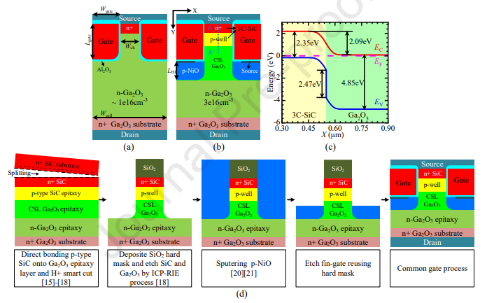
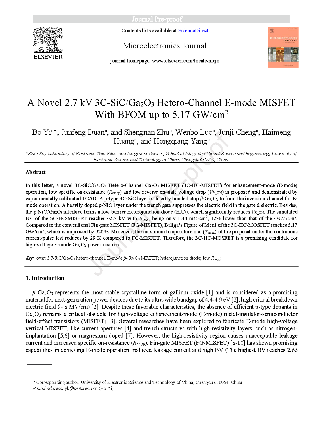
Fig. 1. Schematic cross-sectional view of FG-MISFET and 3C-HC-MISFET. Corner radius of the trench Ga2O3 are set to 0.2 μm. (a) FG-MISFET. (b) 3C-HC-MISFET. (c) Energy band diagram along AA’ in Fig. 1 (b). (d) Possible fabrication process of the 3C-HC-MISFET.
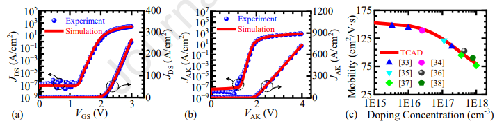
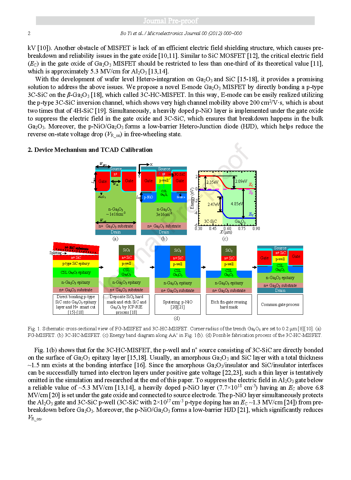
Fig. 2. Calibration of parameters and models based on the measured data. (a) The logarithmic and linear scale calibration of FG-MISFET. (b) The logarithmic and linear scale calibration of p-NiO/Ga2O3 hetero-junction. (c) The calibration of Arora mobility model.
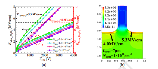
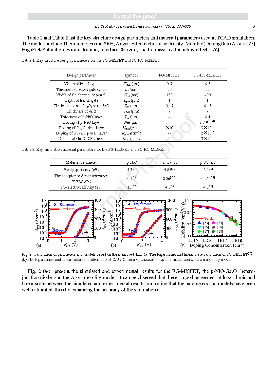
Fig. 3. Maximum electric field (Emax) for different materials in FG-MISFET. (a) Influence of Ndrift on the Emax of Al2O3 and Ga2O3. (b) The electric field distribution at BV = 2000 V, Ndrift = 1×1016 cm-3.
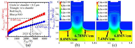
Fig. 4. Effect of corner radius in Ga2O3 trench on the Emax of 3C-HC-MISFET. (a) Emax vs VDS of 3C-HC-MISFET. (b) Electric field distribution of 3C-HC-MISFET with 0.2 μm corner radius VDS = 2725 V. (c) Electric field distribution of 3C-HC-MISFET without corner radius, VDS = 2523 V.
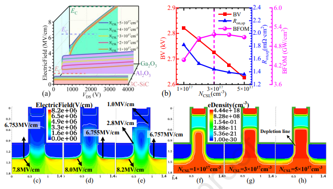
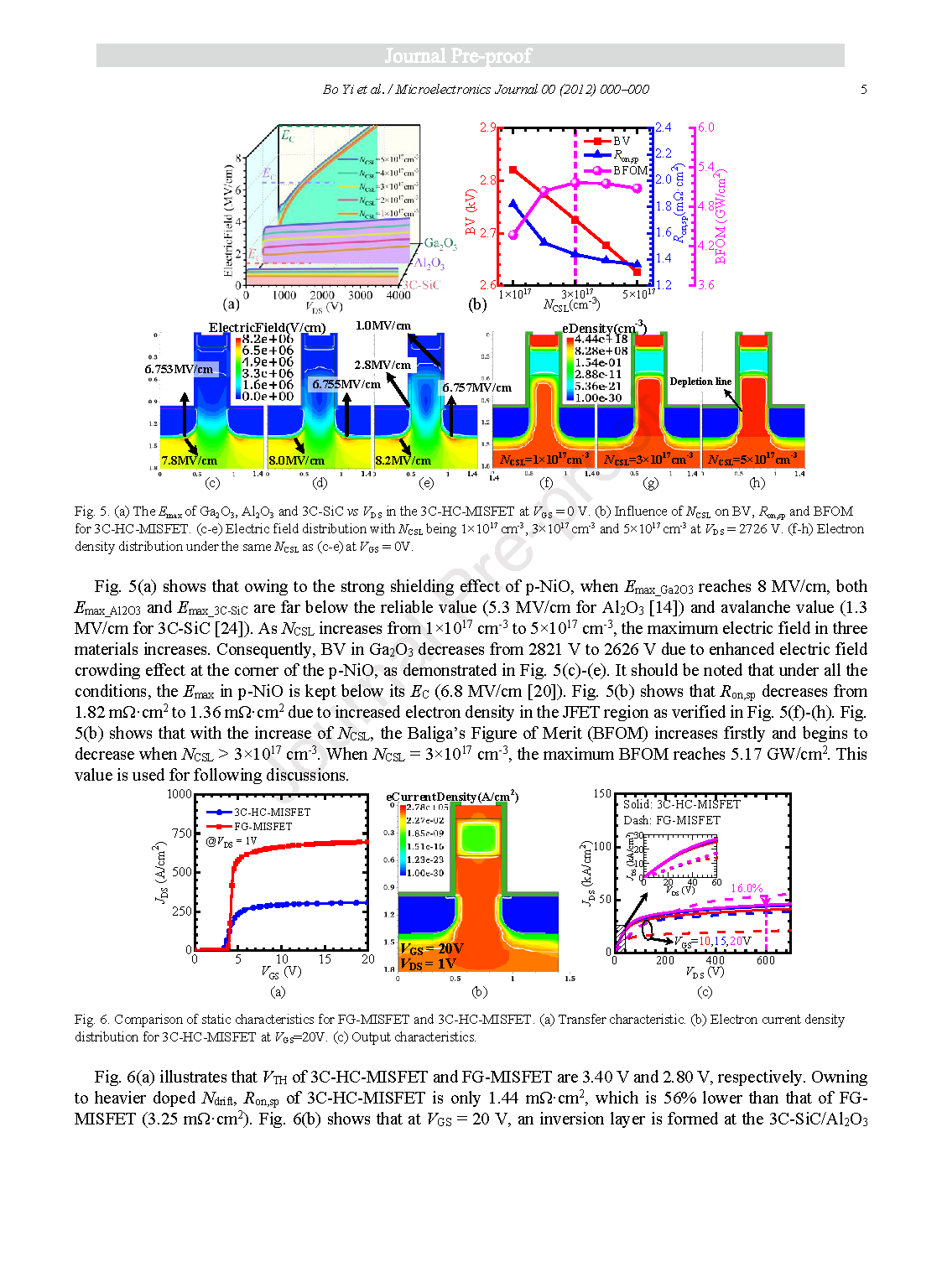
Fig. 5. (a) The Emax of Ga2O3, Al2O3 and 3C-SiC vs VDS in the 3C-HC-MISFET at VGS = 0 V. (b) Influence of NCSL on BV, Ron,sp and BFOM for 3C-HC-MISFET. (c-e) Electric field distribution with NCSL being 1×1017 cm-3, 3×1017 cm-3 and 5×1017 cm-3 at VDS = 2726 V. (f-h) Electron density distribution under the same NCSL as (c-e) at VGS = 0V.
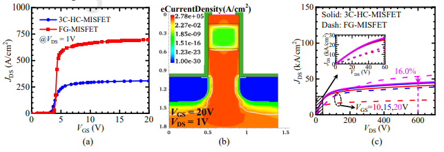
Fig. 6. Comparison of static characteristics for FG-MISFET and 3C-HC-MISFET. (a) Transfer characteristic. (b) Electron current density distribution for 3C-HC-MISFET at VGS=20V. (c) Output characteristics.
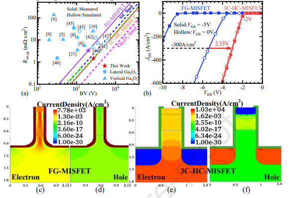
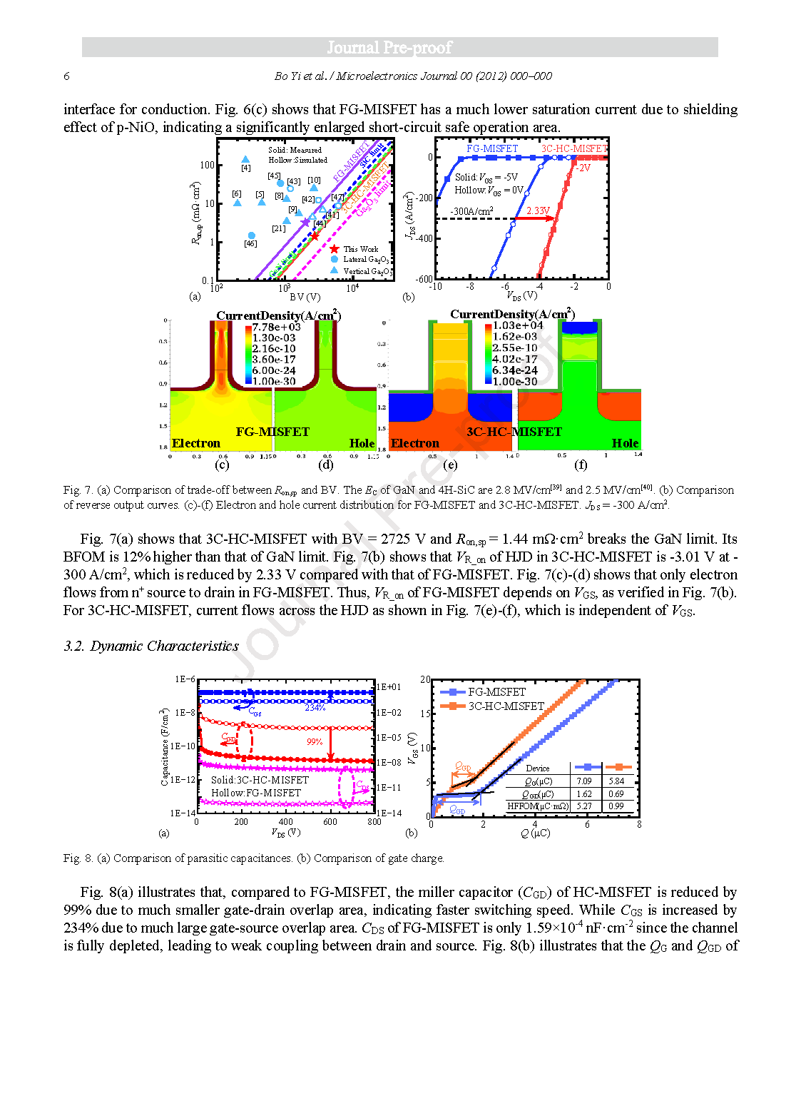
Fig. 7. (a) Comparison of trade-off between Ron,sp and BV. The EC of GaN and 4H-SiC are 2.8 MV/cm and 2.5 MV/cm. (b) Comparison of reverse output curves. (c)-(f) Electron and hole current distribution for FG-MISFET and 3C-HC-MISFET. JDS = -300 A/cm2.
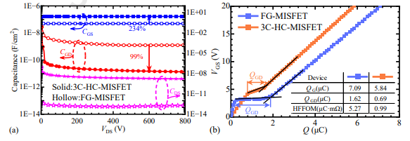
Fig. 8. (a) Comparison of parasitic capacitances. (b) Comparison of gate charge.
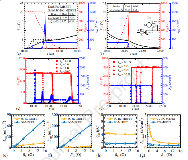
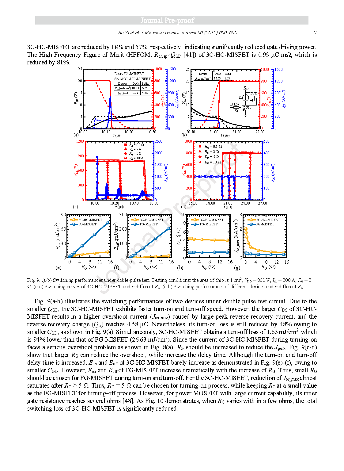
Fig. 9. (a-b) Switching performances under doble-pulse test. Testing conditions: the area of chip is 1 cm2, VDD = 800 V, Idc = 200 A, RG = 2 Ω. (c-d) Switching curves of 3C-HC-MISFET under different RG. (e-h) Switching performances of different devices under different RG.
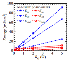
Fig. 10. Switching loss of 3C-HC-MISFET under different RG.
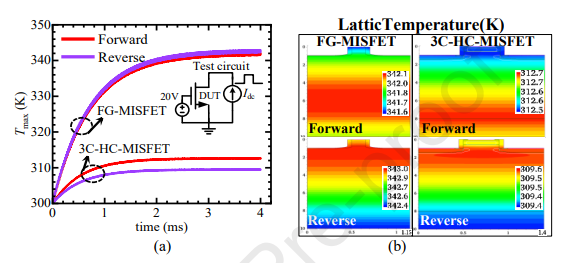
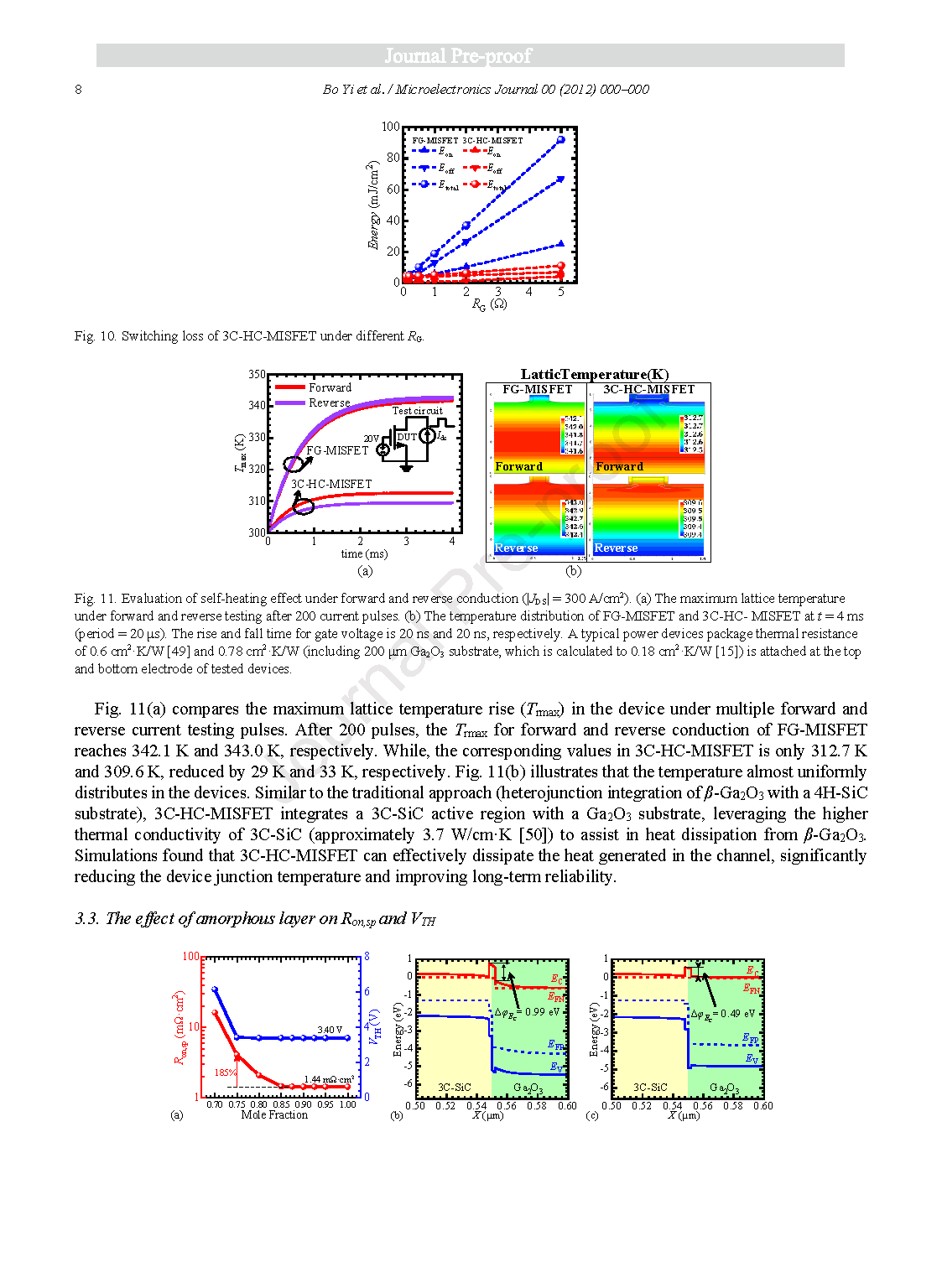
Fig. 11. Evaluation of self-heating effect under forward and reverse conduction (|JDS| = 300 A/cm2). (a) The maximum lattice temperature under forward and reverse testing after 200 current pulses. (b) The temperature distribution of FG-MISFET and 3C-HC- MISFET at t = 4 ms (period = 20 μs). The rise and fall time for gate voltage is 20 ns and 20 ns, respectively. A typical power devices package thermal resistance of 0.6 cm2 ·K/W and 0.78 cm2 ·K/W (including 200 μm Ga2O3 substrate, which is calculated to 0.18 cm2 ·K/W) is attached at the top and bottom electrode of tested devices.
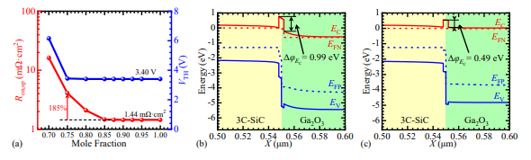
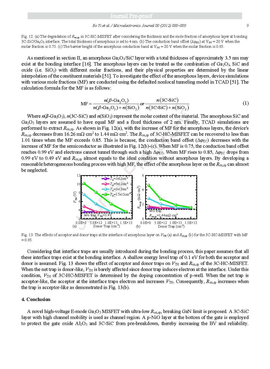
Fig. 12. (a) The degradation of Ron,sp in 3C-HC-MISFET after considering the thickness and the mole fraction of amorphous layer at bonding 3C-SiC/Ga2O3 interface. The total thickness of amorphous is set to 4 nm. (b) The conduction band offset (ΔφEC) at VGS = 20 V when the molar fraction is 0.75. (c) The barrier height of the amorphous conduction band at VGS = 20 V when the molar fraction is 0.85.
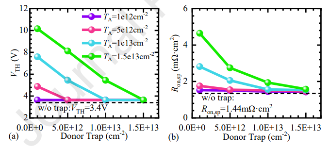
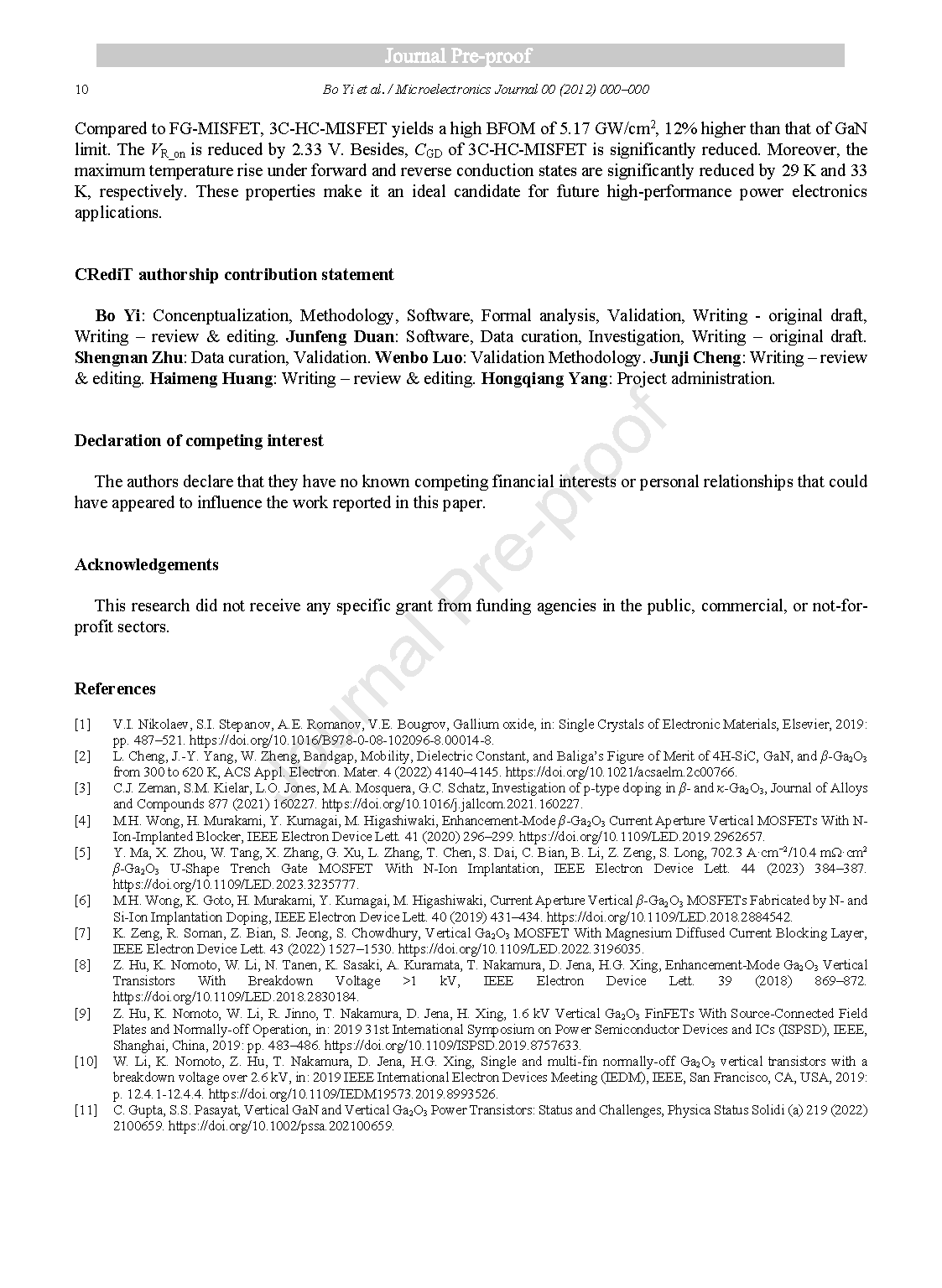
Fig. 13. The effects of acceptor and donor traps at the interface of amorphous layer on VTH (a) and Ron,sp (b) for the 3C-HC-MISFET with MF = 0.85.
DOI:
doi.org/10.1016/j.mejo.2025.106955