


Member News
【Member News】GAREN SEMI Launches (011) β-Ga₂O₃ Substrates, Unlocking a New Era for Power Devices
日期:2025-11-10阅读:620
As the global energy structure transitions and electronic devices upgrade to high power and high reliability, fourth-generation semiconductor materials have become the focus of the industry with their outstanding performance. Among them, Gallium Oxide, with its unique advantages of an ultra-wide bandgap of 4.9eV and a high breakdown electric field of 8MV/cm, is regarded as the "key material" to solve the pain points of high-voltage, high-frequency and high-temperature application scenarios. In November 2025, Hangzhou GAREN SEMI Co., LTD. (hereinafter referred to as "GAREN SEMI"), relying on its profound technological accumulation, officially launched the new product (011) crystal plane Gallium Oxide substrate, continuously providing core support for industrial breakthroughs.
1.Core Performance Maximized — Redefining Substrate Quality
The new β-Ga2O3 (011) crystal plane substrate is available in two precise sizes: 10mm*10.5mm and 10mm*15mm, with short side positioning [100] crystal orientation, providing a more stable foundation for device fabrication.
In terms of key performance indicators, the product has achieved a comprehensive breakthrough:
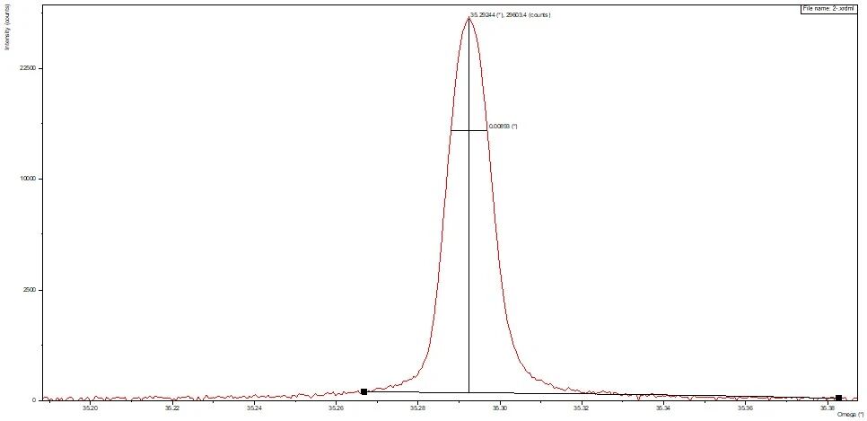
Outstanding Performance Testing
A 10 mm × 10.5 mm (011) crystal-oriented substrate exhibits a double-crystal rocking curve full width at half maximum (FWHM) of only 32.1 arc sec in XRD measurements, indicating a highly concentrated crystal orientation distribution. The peak position is 35.29°, very close to the theoretical value of 35.148°. This excellent performance fundamentally ensures the long-term operational stability of devices.
Top Surface Quality
The substrate wafer achieves industry-leading surface quality, featuring an ultra-smooth surface with an Ra value below 0.5 nm and crystal orientation deviation strictly controlled within ±1°. It also offers single- or double-sided polishing options, providing an ideal platform for epitaxial growth.
Wide Variety of Customization Types
(011) crystal plane substrates offer a variety of doping and carrier concentration options. Currently, three doping types - UID, Sn, and Mg/Fe - are available to meet the design requirements of diverse devices.
Behind each parameter lies GAREN SEMI's ultimate pursuit of process details, ensuring that downstream customers do not have to compromise in the research and development of high-power and high-precision devices.
2. (011) Crystal Face Stands Out, Leading a New Direction in Industrial Development
As an innovative crystal plane option in the field of Gallium Oxide materials, the (011) crystal plane offers multiple irreplaceable advantages that are set to reshape the future landscape of industrial applications:
Stronger Defect Suppression
The (011) crystal plane structure naturally avoids linear defects, reducing issues such as electric field concentration and reverse current. This significantly enhances the breakdown performance and service life of power devices, making it especially suitable for ultra-high-voltage applications.
Better Electrical Contact Performance
The surface barrier height of the (011) crystal plane is lower than that of the conventional (001) plane, facilitating low-resistance ohmic contacts and reducing device conduction loss. This provides critical support for high-efficiency applications, including 5G base station power supplies and ultra-high-voltage power transmission and transformation equipment.
Wider Epitaxial Compatibility
The (011) crystal plane has a lattice mismatch of less than 1.5% with multi-component solid solutions such as AlGaO and InGaO, enabling stable growth of high-quality epitaxial layers. This lays a foundation for developing advanced devices such as multi-band deep-ultraviolet photodetectors and quantum-well lasers.
3.Innovation Never Stops, Showcasing Core Scientific Strength
The successful development of the (011) crystal plane substrate is no accident—it is the inevitable result of GAREN SEMI’s long-term technological accumulation. Leveraging its independently developed casting method with proprietary intellectual property and self-designed crystal growth equipment dedicated to Gallium Oxide, the company has targeted key industry challenges and successfully achieved stable growth across multiple sizes and crystal faces, along with breakthroughs in conductive doping. This demonstrates the company’s continuous innovative “Gallium speed.”
In 2025, GAREN SEMI set an industry record by iterating substrate sizes from 2 inches to 8 inches at a rate of one new size per year. Remarkably, it also achieved a breakthrough in the VB method, progressing from zero to 6-inch single crystals in just one year—effectively filling domestic gaps in the field and providing crucial support for the localization of fourth-generation semiconductor materials in China.

The launch of the (011) crystal plane substrate further enriches GAREN SEMI’s Gallium Oxide product matrix and validates the company’s full-chain technical capabilities across crystal growth, process optimization, and performance control. From laboratory research to industrial production, GAREN SEMI continues to drive technological breakthroughs that empower the development of the fourth-generation semiconductor industry, strengthening China’s position in the global semiconductor landscape.
The new (011) crystal plane substrate is now available for sample requests and partnership inquiries. GAREN SEMI warmly invites research institutions and device manufacturers to collaborate and explore the full potential of Gallium Oxide, jointly creating new value for the semiconductor industry.
For more information about GAREN SEMI and its products
Visit our official website: http://garen.cc/
Or contact us in the following ways:
Mr. Jiang :15918719807
Email :jiangjiwei@garen.cc
Mr. Xia :19011278792
Email :xianing@garen.cc
