Paper Sharing
【International Papers】Enhanced mobility and bias stability of SnO₂ thin-film transistors enabled by Ga₂O₃ passivation-induced two-dimensional electron gas
日期:2025-10-20阅读:495
Researchers from the Kyungpook National University have published a dissertation titled "Enhanced mobility and bias stability of SnO2 thin-film transistors enabled by Ga2O3 passivation-induced two-dimensional electron gas" in Materials Today Advances.
Background
Thin-film transistors (TFTs) are essential components that control each pixel in active-matrix displays, such as organic light-emitting diode (OLED) displays and liquid crystal displays (LCDs). Amorphous-phase hydrogenated silicon (a-Si:H) TFTs and polycrystalline silicon (poly-Si) TFTs, fabricated at low temperatures, have been widely employed. However, in recent decades, metal oxide-based TFTs have emerged as fundamental components in active-matrix displays and have replaced their predecessors because they provide higher field-effect mobility than amorphous-phase hydrogenated silicon and exhibit lower leakage currents than low-temperature polycrystalline silicon (poly-Si). In addition, their larger optical bandgap results in transparency, which makes them promising for transparent electronics. As a result, metal oxide-based TFTs are being explored for next-generation display, rollable, and flexible electronic applications.
Historically, ZnO and In2O3 have been investigated as active channel layers in TFTs. Compared with these, SnO2 offers distinct advantages. The intrinsic carrier mobility and transparency of SnO2 are higher than those of ZnO or In2O3. In addition, SnO2 has a lower melting point, which means that the sintering temperature required for high crystallinity is lower than that of ZnO and In2O3. This represents a critical advantage for achieving low-temperature processing with SnO2. According to the United States Geological Survey, the global refined production of indium (In), zinc (Zn), and tin (Sn) in 2024 was approximately 990 tons, 12,000 tons, and 290,000 tons, respectively. This supply difference further strengthens the push to replace In and Zn in device applications.
Abstract
This study presents a method to achieve both high performance and electrical stability in SnO2 thin-film transistors (TFTs) fabricated by a sol–gel process. Sol–gel–processed Ga2O3 passivation layers are introduced onto the SnO2 active channel layers to address bias instabilities. The Ga2O3 films passivate the back channel by compensating dangling bonds and isolating the channel from H2O and O2, which improves bias stability. Structural, optical, chemical, and device-level properties were systematically analyzed. When Ga2O3 is deposited on SnO2, electrons redistribute to maintain thermal equilibrium and become confined in the potential well of SnO2, forming a quasi two-dimensional electron gas that increases the free carrier concentration. This effect results in a 1.5-fold enhancement in field-effect mobility (from ∼10 cm2/Vs to ∼15 cm2/Vs) together with improved bias stability. The proposed SnO2–Ga2O3 passivation method offers a promising route toward bias-stable, high-performance metal oxide films for applications in TFTs, solar cells, transparent conducting electrodes, and resistive random-access memory (ReRAM).
Highlights
● Sol-gel processed SnO2/G2O3 hetero structure were introduced for metal oxide thin film transistors.
● The deposited Ga2O3 films effectively passivate the back channel of the TFTs, leading to bias stability of TFTs.
● A-quasi two-dimensional electron gas was formed in the potential well of SnO2 due to lower work function of Ga2O3.
● The increased carrier concentration results in enhancement in field effect mobility simultaneously.
Conclusion
This work demonstrates a strategy to achieve both high performance and electrical stability in metal oxide thin-film transistors through the introduction of Ga2O3 passivation layers into sol–gel–processed SnO2 TFTs. The Ga2O3 layers effectively suppress oxygen vacancies at the SnO2 surface because Ga-O bonds are stronger than Sn-O bonds. They also minimize unwanted surface reactions such as oxygen adsorption and desorption caused by ambient gases, both of which are critical factors in bias stability.
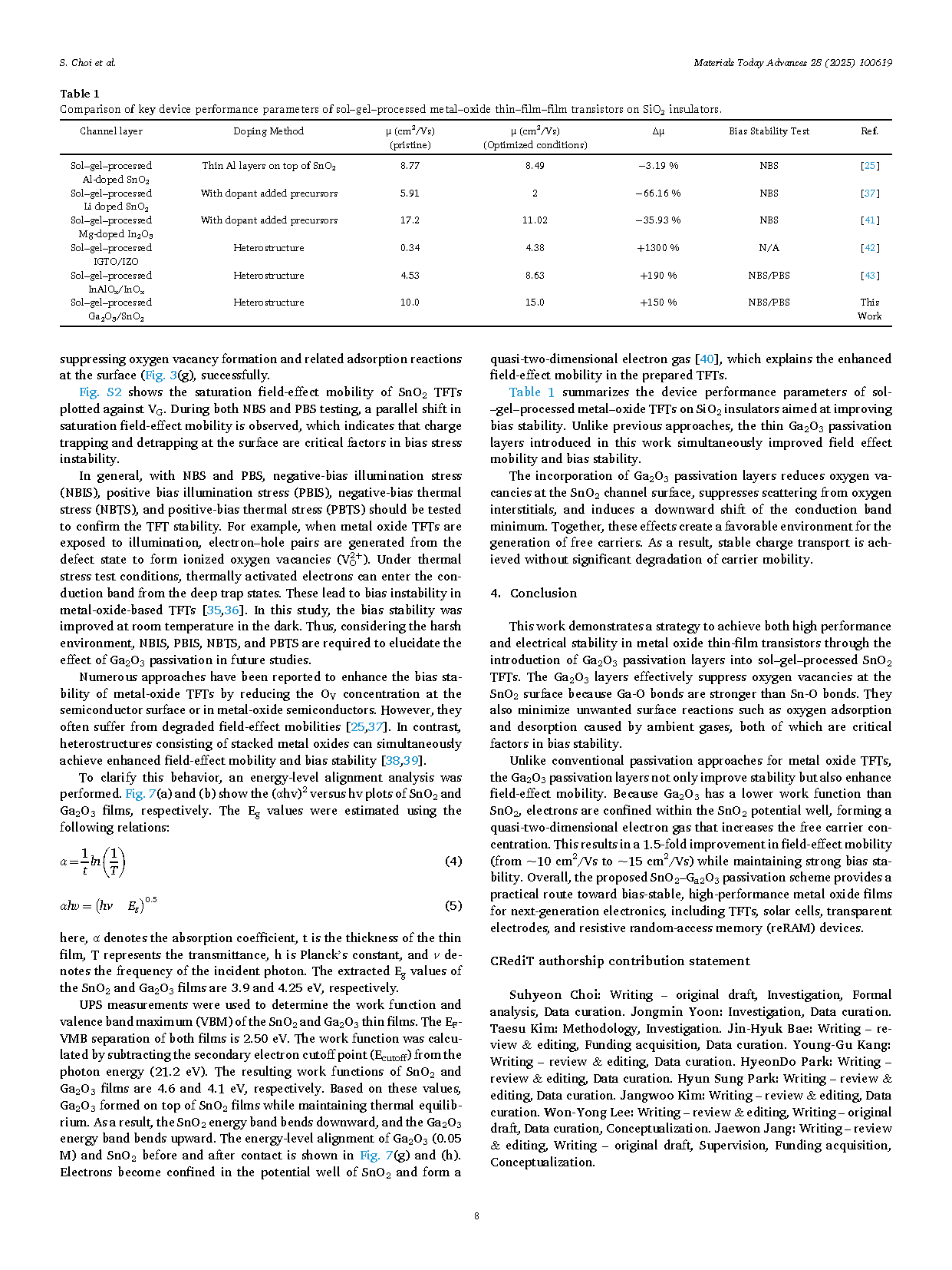
Unlike conventional passivation approaches for metal oxide TFTs, the Ga2O3 passivation layers not only improve stability but also enhance field-effect mobility. Because Ga2O3 has a lower work function than SnO2, electrons are confined within the SnO2 potential well, forming a quasi-two-dimensional electron gas that increases the free carrier concentration. This results in a 1.5-fold improvement in field-effect mobility (from ∼10 cm2/Vs to ∼15 cm2/Vs) while maintaining strong bias stability. Overall, the proposed SnO2–Ga2O3 passivation scheme provides a practical route toward bias-stable, high-performance metal oxide films for next-generation electronics, including TFTs, solar cells, transparent electrodes, and resistive random-access memory (reRAM) devices.
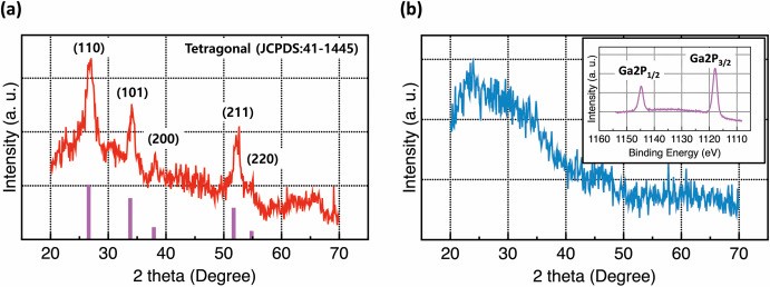
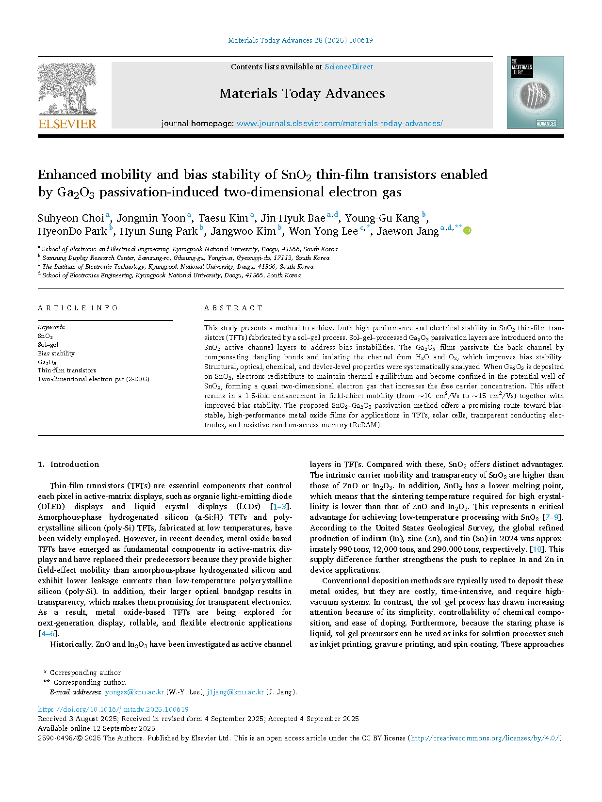
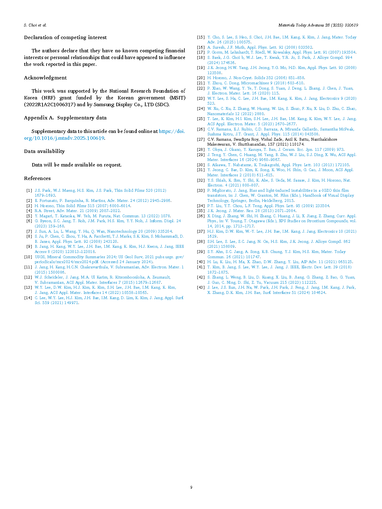
Fig. 1. GIXRD spectra of the (a) single SnO2 films and (b) single Ga2O3 films. The inset shows high-resolution XPS spectra of Ga 2p.
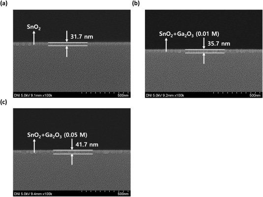
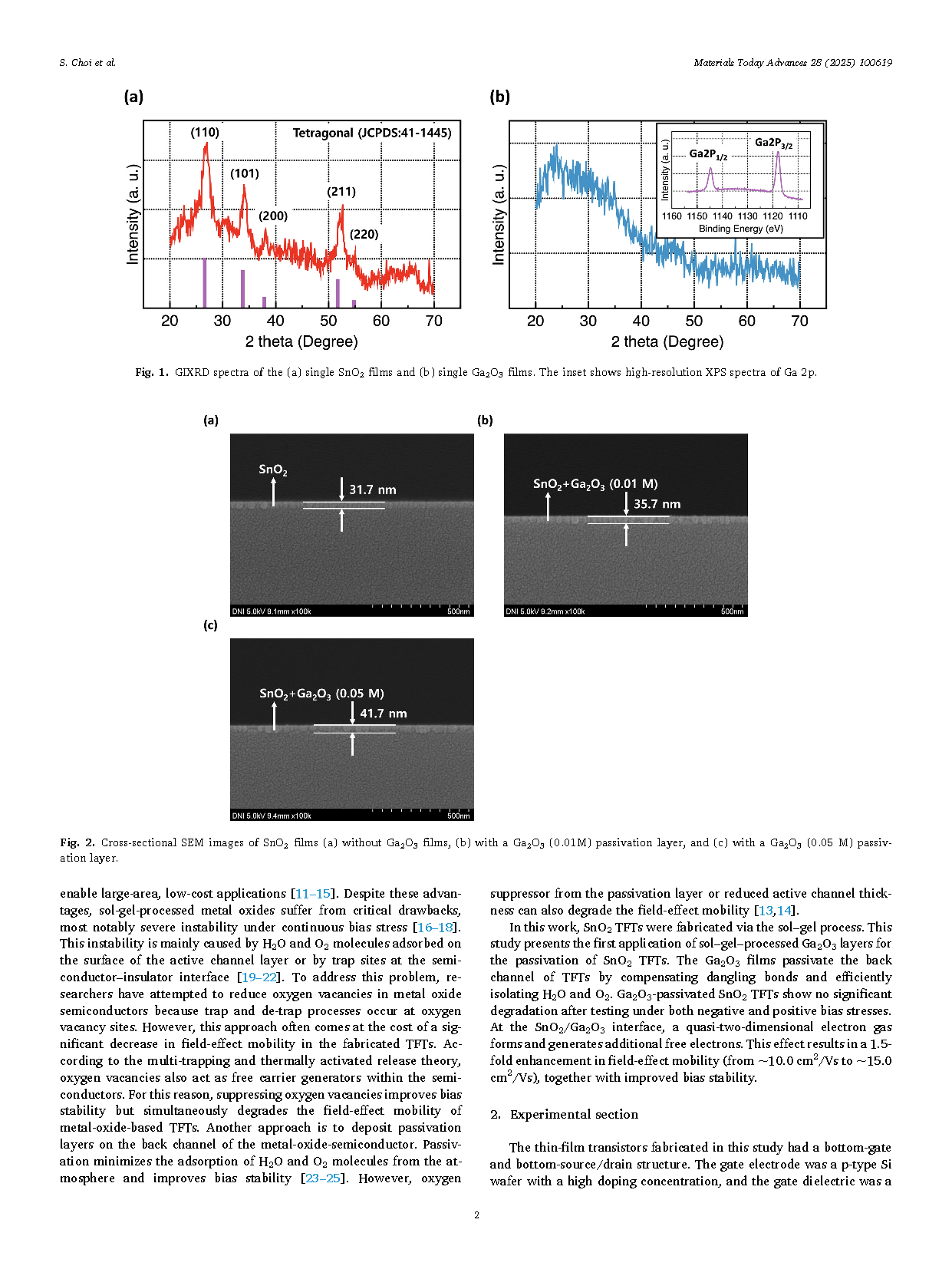
Fig. 2. Cross-sectional SEM images of SnO2 films (a) without Ga2O3 films, (b) with a Ga2O3 (0.01M) passivation layer, and (c) with a Ga2O3 (0.05 M) passivation layer.
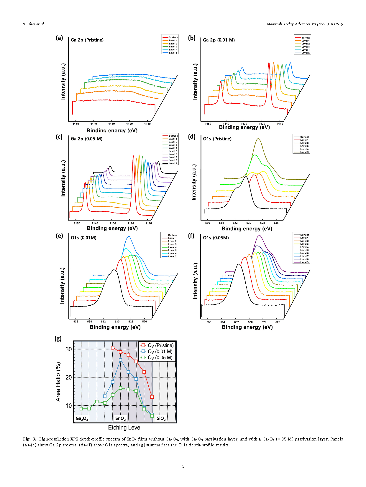
Fig. 3. High-resolution XPS depth-profile spectra of SnO2 films without Ga2O3, with Ga2O3 passivation layer, and with a Ga2O3 (0.05 M) passivation layer. Panels (a)–(c) show Ga 2p spectra, (d)–(f) show O1s spectra, and (g) summarizes the O 1s depth-profile results.
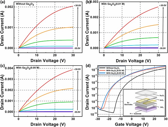
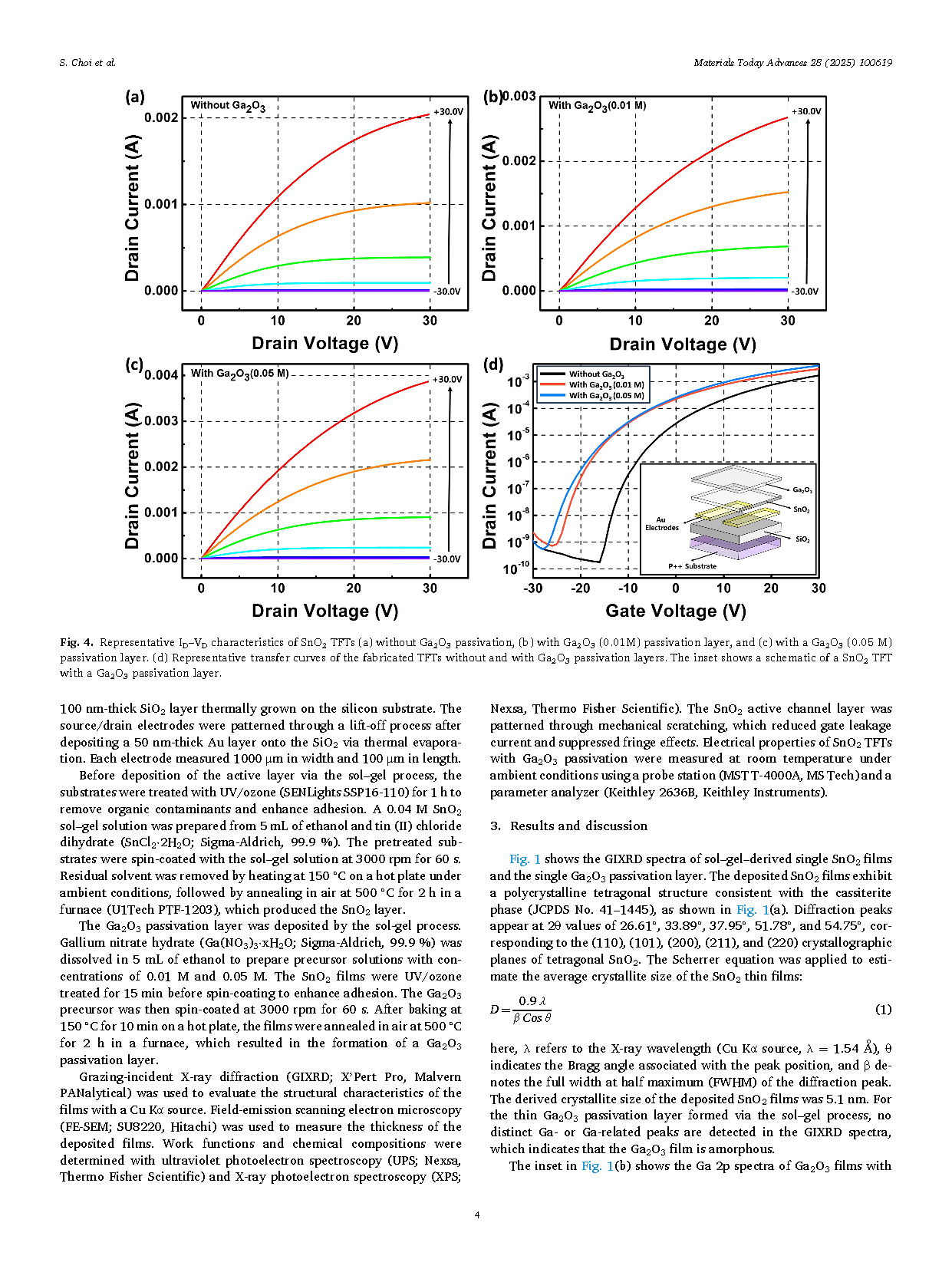
Fig. 4. Representative ID–VD characteristics of SnO2 TFTs (a) without Ga2O3 passivation, (b) with Ga2O3 (0.01M) passivation layer, and (c) with a Ga2O3 (0.05 M) passivation layer. (d) Representative transfer curves of the fabricated TFTs without and with Ga2O3 passivation layers. The inset shows a schematic of a SnO2 TFT with a Ga2O3 passivation layer.
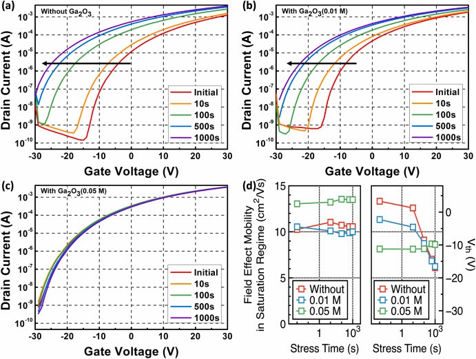
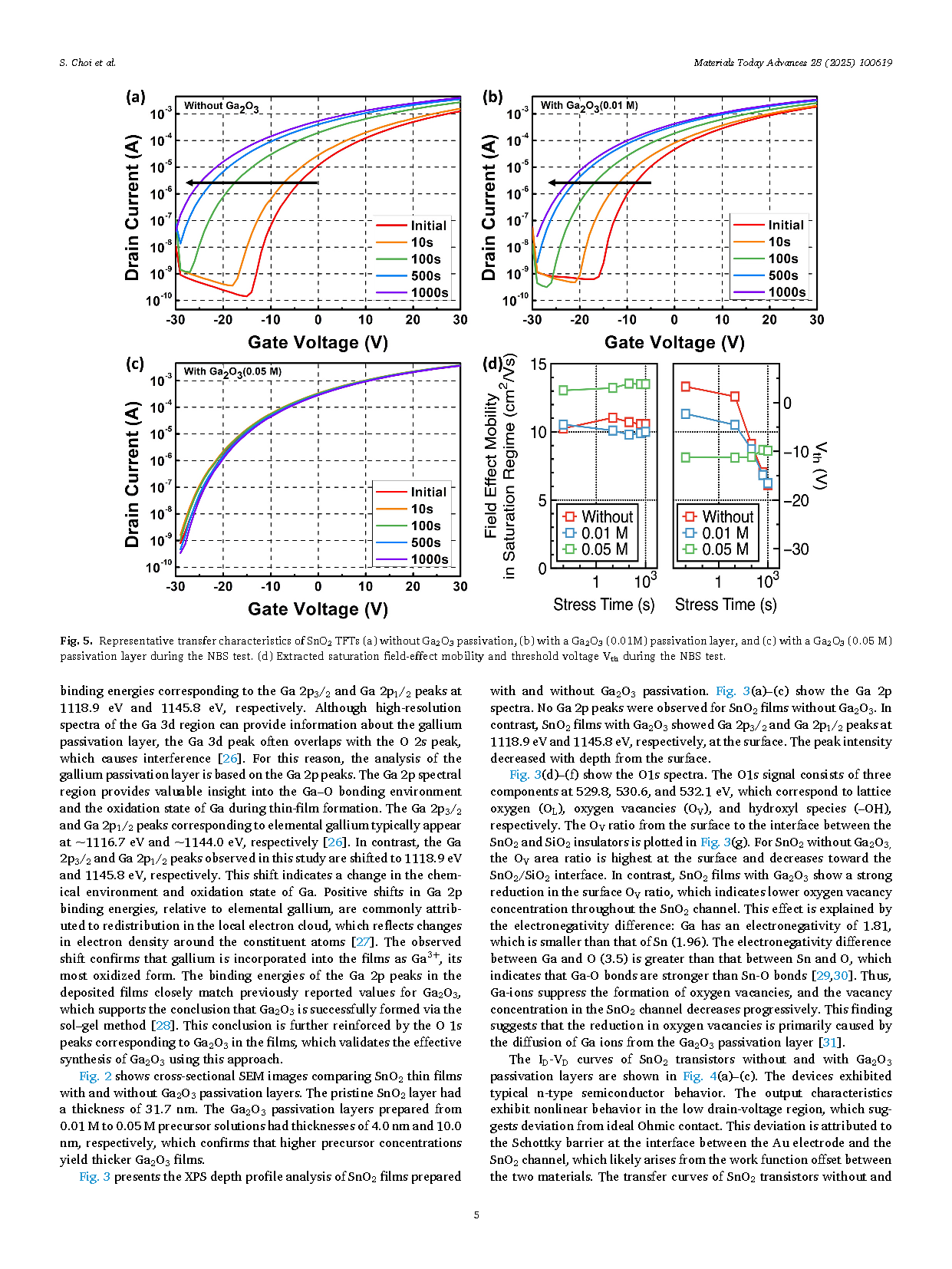
Fig. 5. Representative transfer characteristics of SnO2 TFTs (a) without Ga2O3 passivation, (b) with a Ga2O3 (0.01M) passivation layer, and (c) with a Ga2O3 (0.05 M) passivation layer during the NBS test. (d) Extracted saturation field-effect mobility and threshold voltage Vth during the NBS test.
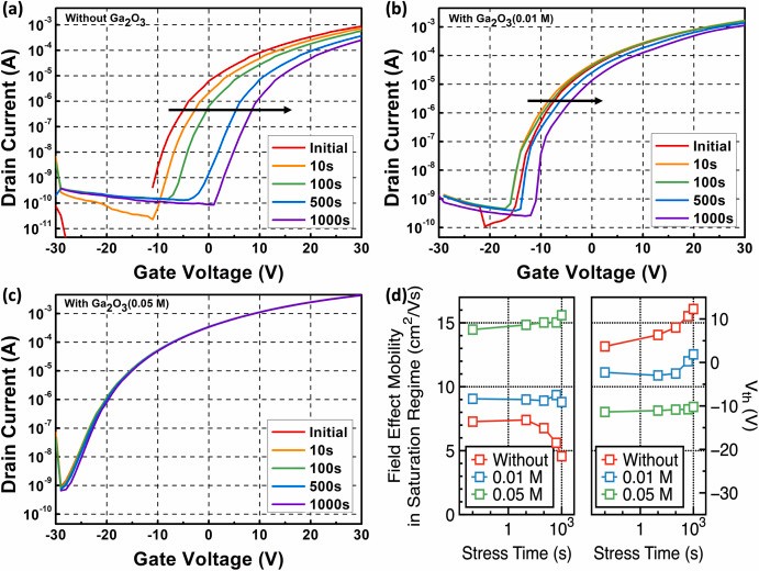
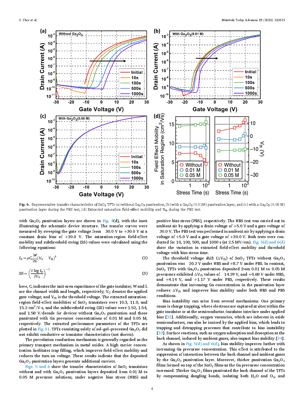
Fig. 6. Representative transfer characteristics of SnO2 TFTs (a) without Ga2O3 passivation, (b) with a Ga2O3 (0.01M) passivation layer, and (c) with a Ga2O3 (0.05 M) passivation layer during the PBS test, (d) Extracted saturation field-effect mobility and Vth during the PBS test.
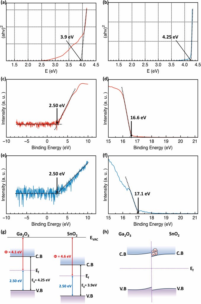
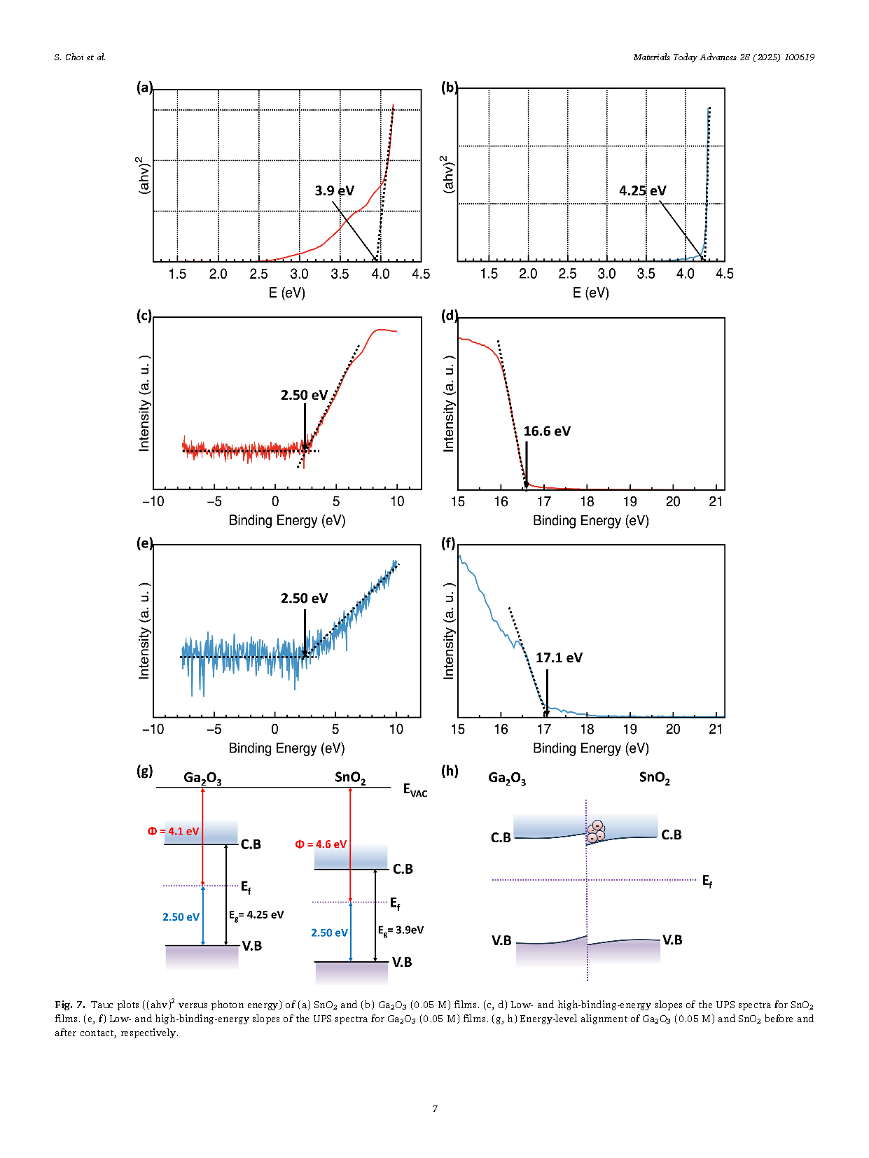
Fig. 7. Tauc plots ((ahv)2 versus photon energy) of (a) SnO2 and (b) Ga2O3 (0.05 M) films. (c, d) Low- and high-binding-energy slopes of the UPS spectra for SnO2 films. (e, f) Low- and high-binding-energy slopes of the UPS spectra for Ga2O3 (0.05 M) films. (g, h) Energy-level alignment of Ga2O3 (0.05 M) and SnO2 before and after contact, respectively.
DOI:
doi.org/10.1016/j.mtadv.2025.100619