Paper Sharing
【Domestic Papers】Single-event burnout in β-Ga₂O₃ Schottky barrier diode induced by heavy ion irradiation
日期:2025-10-10阅读:489
Researchers from the China Electronic Product Reliability and Environmental Testing Research Institute have published a dissertation titled "Single-event burnout in β-Ga2O3 Schottky barrier diode induced by heavy ion irradiation" in Applied Physics Letters.
Project Support
This work was supported in part by the National Natural Science Foundation of China under Grant No. 12305299 and in part by the Xinjiang Uygur Autonomous Region 2023 “Tianchi YingCai Program” under Grant No. 2024000057.
Background
Beta-phase gallium oxide (β-Ga2O3) has attracted significant attention for electronic device applications due to its outstanding material properties. With an ultra-wide bandgap of 4.9 eV and a high critical electric field strength of up to 8 MV/cm, β-Ga2O3 offers remarkable advantages for high-temperature and high-power electronic devices, such as power rectifiers, deep-ultraviolet photodetectors, and metal–oxide–semiconductor field-effect transistors (MOSFETs). In addition, β-Ga2O3 can be grown by melt-based methods, which are more cost-effective than those used for SiC and GaN, further promoting its development in high-power electronics.
Abstract
This study investigates single-event burnout (SEB) effects in β-Ga2O3 Schottky barrier diodes under heavy ion irradiation. Bi, Ta, and Kr ions with linear energy transfer (LET) values of 99.7, 75, and 37 MeV/(mg·cm2), respectively, were used in the experiments. The results show that the SEB threshold voltage decreases with increasing LET, indicating a strong dependence on energy deposition. In addition, reverse bias is identified as a critical triggering condition for SEB, which occurs only when the applied voltage is high enough to initiate thermal runaway and cause irreversible damage. To further elucidate the failure mechanism, Kr ions were selected for detailed investigation. technology computer-aided design simulations combined with scanning electron microscopy-based failure analysis revealed that transient current surges can rapidly elevate the local temperature. Once the temperature reaches the melting point of Ga2O3 material, SEB is triggered by irreversible thermal failure. Moreover, the failure sites were primarily located at the edge of the Schottky junction, indicating structural vulnerability in this region. These findings clarify the LET and reverse bias dependence of SEB in ultra-wide bandgap devices and provide insights into radiation-hardened design.
Conclusion
In summary, this study systematically investigates the physical mechanism of SEB induced by heavy ion irradiation in b-Ga2O3 SBD by combining experimental testing with TCAD simulations under various LET conditions. The results show that SEB triggering depends not only on the LET of the incident ions but also strongly on the magnitude of the applied reverse bias. High-LET ions tend to induce SEB at lower voltages due to concentrated energy deposition, while lowerLET ions require higher bias to reach the critical failure threshold. The EMMI analysis confirms that the burnout site is located at the edge of the Schottky junction. Further FIB-SEM analysis reveals that the thermal runaway during the SEB process causes catastrophic structural damage, extending beyond the epitaxial layer and partially into the substrate, resulting in a distinct vertical burnout path. These findings provide insights for improving the thermal robustness and radiation tolerance of Ga2O3-based power devices operating in harsh environments.
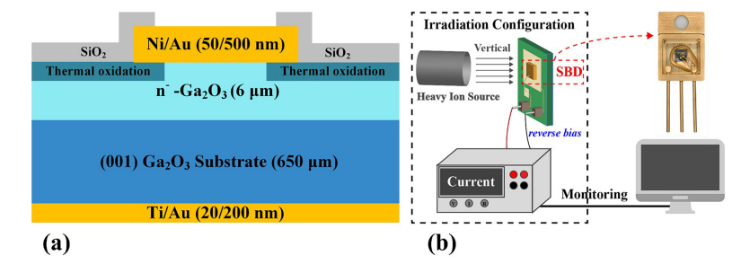
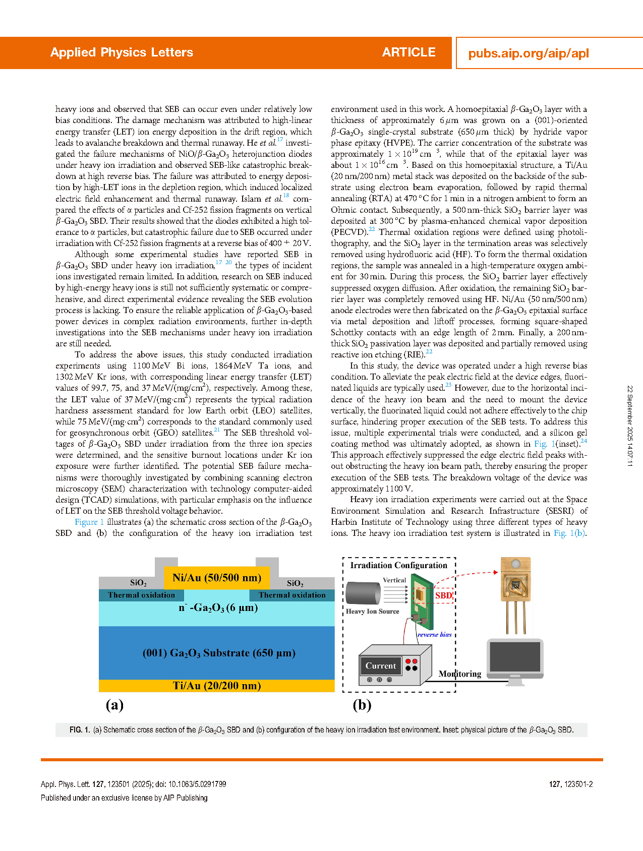
FIG. 1. (a) Schematic cross section of the β-Ga2O3 SBD and (b) configuration of the heavy ion irradiation test environment. Inset: physical picture of the β-Ga2O3 SBD.
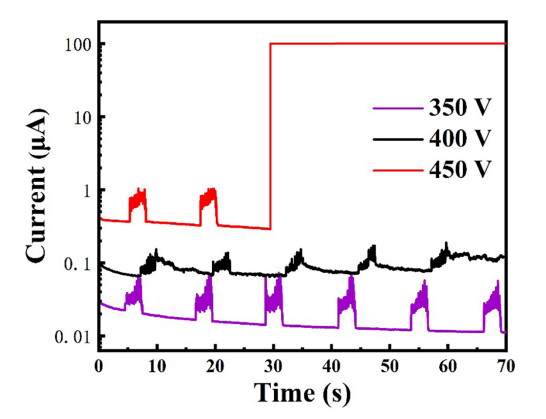
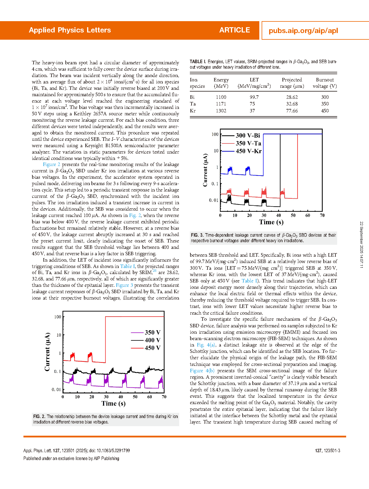
FIG. 2. The relationship between the device leakage current and time during Kr ion irradiation at different reverse bias voltages.
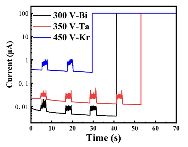
FIG. 3. Time-dependent leakage current curves of β-Ga2O3 SBD devices at their respective burnout voltages under different heavy ion irradiations.
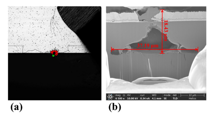
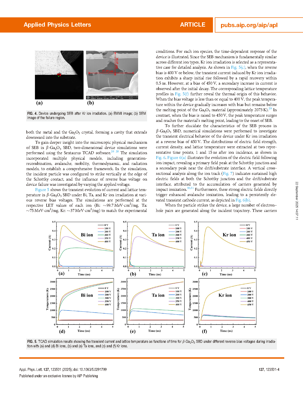
FIG. 4. Device undergoing SEB after Kr ion irradiation. (a) EMMI image; (b) SEM image of the failure region.
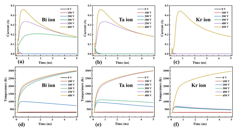
FIG. 5. TCAD simulation results showing the transient current and lattice temperature as functions of time for β-Ga2O3 SBD under different reverse bias voltages during irradiation with (a) and (d) Bi ions, (b) and (e) Ta ions, and (c) and (f) Kr ions.
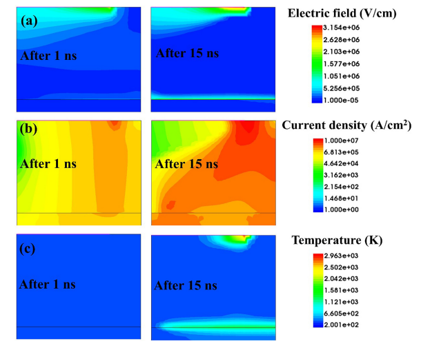
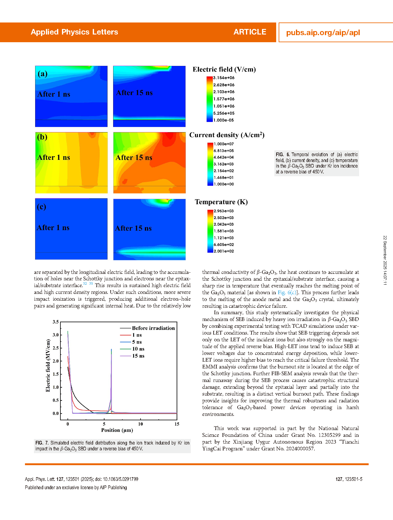
FIG. 6. Temporal evolution of (a) electric field, (b) current density, and (c) temperature in the β-Ga2O3 SBD under Kr ion incidence at a reverse bias of 450 V.
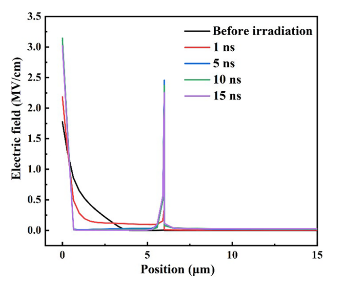
FIG. 7. Simulated electric field distribution along the ion track induced by Kr ion impact in the β-Ga2O3 SBD under a reverse bias of 450 V.
DOI:
doi.org/10.1063/5.0291799