Paper Sharing
【Member Papers】Structural and optical properties of high crystalline quality orthorhombic к-Ga₂O₃ heteroepitaxial films grown by HVPE
日期:2025-09-28阅读:525
Researchers from the Tianjin University of Technology have published a dissertation titled "Structural and optical properties of high crystalline quality orthorhombic к-Ga2O3 heteroepitaxial films grown by HVPE" in Applied Physics A.
Project Support
This work was supported by the Major Project of Tianjin Science and Technology (Grant No. 18ZXJMTG00230) and the Key Research and Development Program of Tianjin (Nos. 24YFXTHZ00200 and 24YFXTHZ00210).
Background
Gallium oxide (Ga2O3) has become a pivotal material in next-generation power electronics and deep-ultraviolet (UV) optoelectronics because of its exceptional properties: an ultrawide bandgap (4.6–5.3 eV), a high breakdown electric field (>8 MV/cm), excellent optical transparency, and robust chemical stability. Ga2O3 exhibits multiple polymorphs, including the α-, β-, γ-, δ- and κ-Ga2O3 phases. Although the most thermodynamically stable monoclinic β-phase has been primarily researched, the orthorhombic κ-phase (space group Pna21) exhibits distinctive performance advantages, such as a high dielectric constant, spontaneous polarization, and piezoelectric properties. These exceptional characteristics enable its use in innovative devices, including high-mobility transistors and piezoelectric sensors.
Abstract
Herein, high crystalline quality orthorhombic κ-Ga2O3 epitaxial films were grown on c-Al2O3 substrates via hydride vapor phase epitaxy. A pure-phase κ-Ga2O3 film deposited at 800 ℃ exhibited exceptional crystalline quality, with a symmetric rocking-curve full width at half maximum of 379″. The out-of-plane epitaxial relationship between the κ-Ga2O3 film and c-Al2O3 substrate was determined to be κ-Ga2O3 (001)//Al2O3 (0001), and the in-plane epitaxial relationships were κ-Ga2O3 [010]//Al2O3 [10_10] and κ-Ga2O3 [110]//Al2O3 [1_100]. The film deposited at 800 ℃ showed an average visible-light transmittance of 70%, an optical bandgap of 4.72 eV. Photoluminescence (PL) spectra show that the films exhibit strong ultraviolet (UV)-green emission in the wavelength range of 300 to 700 nm. The Hall mobility of this film was 25 cm2 V−1 s−1, with a carrier concentration of 3.34 × 1018 cm−3.
Conclusion
Herein, through the optimization of the growth-zone temperature, we prepared high crystalline quality orthorhombic κ-Ga2O3 epitaxial films on c-plane sapphire substrates via HVPE at 800 ℃ and investigated their surface morphology, crystal structure, crystalline quality, and optoelectronic properties. XRD analysis confirms that the sample prepared at 800℃ is a phase-pure κ-Ga2O3 epitaxial film, and it is observed that the epitaxial film undergoes a κ→β phase transition with increasing temperature. SEM characterization reveals that the κ-Ga2O3 epitaxial film exhibits excellent surface morphology. The out-of-plane epitaxial relationship was determined to be κ-Ga2O3 (001)//Al2O3 (0001), and the in-plane relationships were identified to be κ-Ga2O3 [010]//Al2O3 [10_10] and κ-Ga2O3 [110]//Al2O3 [1_100]. Notably, the prepared film showed a symmetric rocking-curve FWHM of 379″. The results of HRTEM and SAED confirmed an ordered atomic arrangement in the film. Furthermore, the film showed an average transmittance in the visible range of 70% and an optical bandgap of 4.72 eV. The Hall mobility of the film was 25 cm2 V−1 s−1, with a carrier concentration of 3.34×1018 cm−3. The comprehensive characterization results provide critical insights into the structural, optical, and electrical properties of the pure-phase metastable κ-Ga2O3 films, laying a foundation for future device applications.
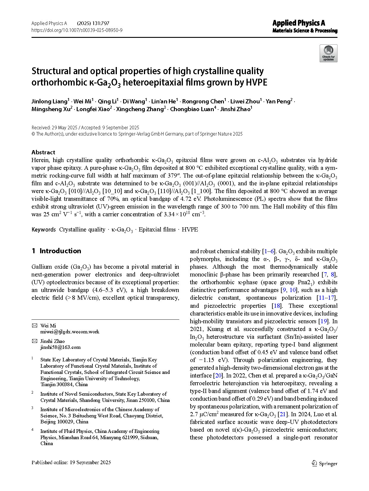
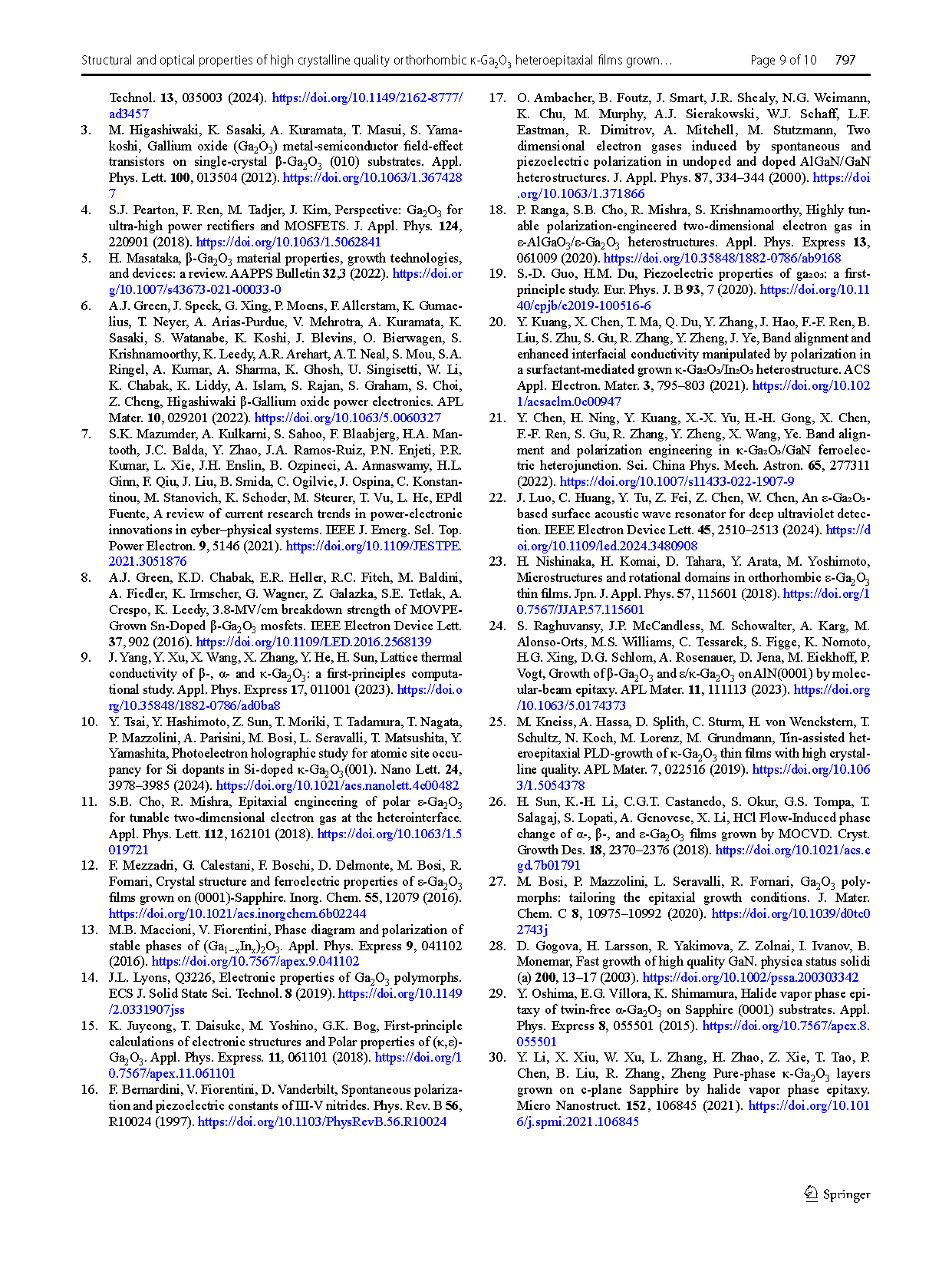
Fig. 1 Schematic diagram of HVPE-based κ-Ga2O3 film growth.
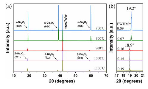
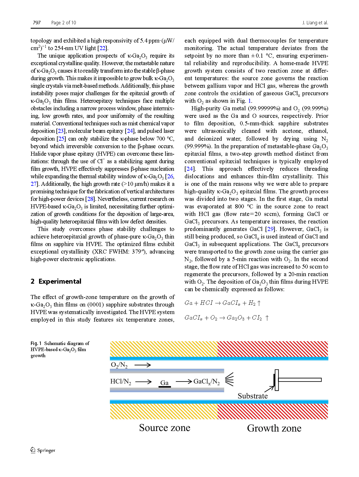
Fig. 2 (a) XRD θ–2θ scan patterns of Ga2O3 epitaxial films grown at different temperatures; (b) Magnified view of the 2θ=17–21° region.
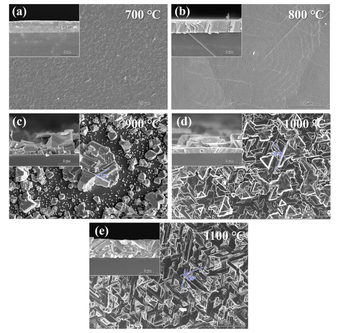
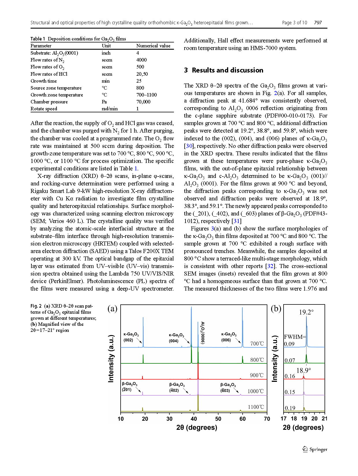
Fig. 3 (a–b) Cross-sectional SEM images of κ-Ga2O3 grown at 700–800 °C, with insets showing corresponding plan-view morphology; (c– e) Cross-sectional SEM images of β-Ga2O3 grown at 800–1000 °C, with insets showing corresponding plan-view morphology.

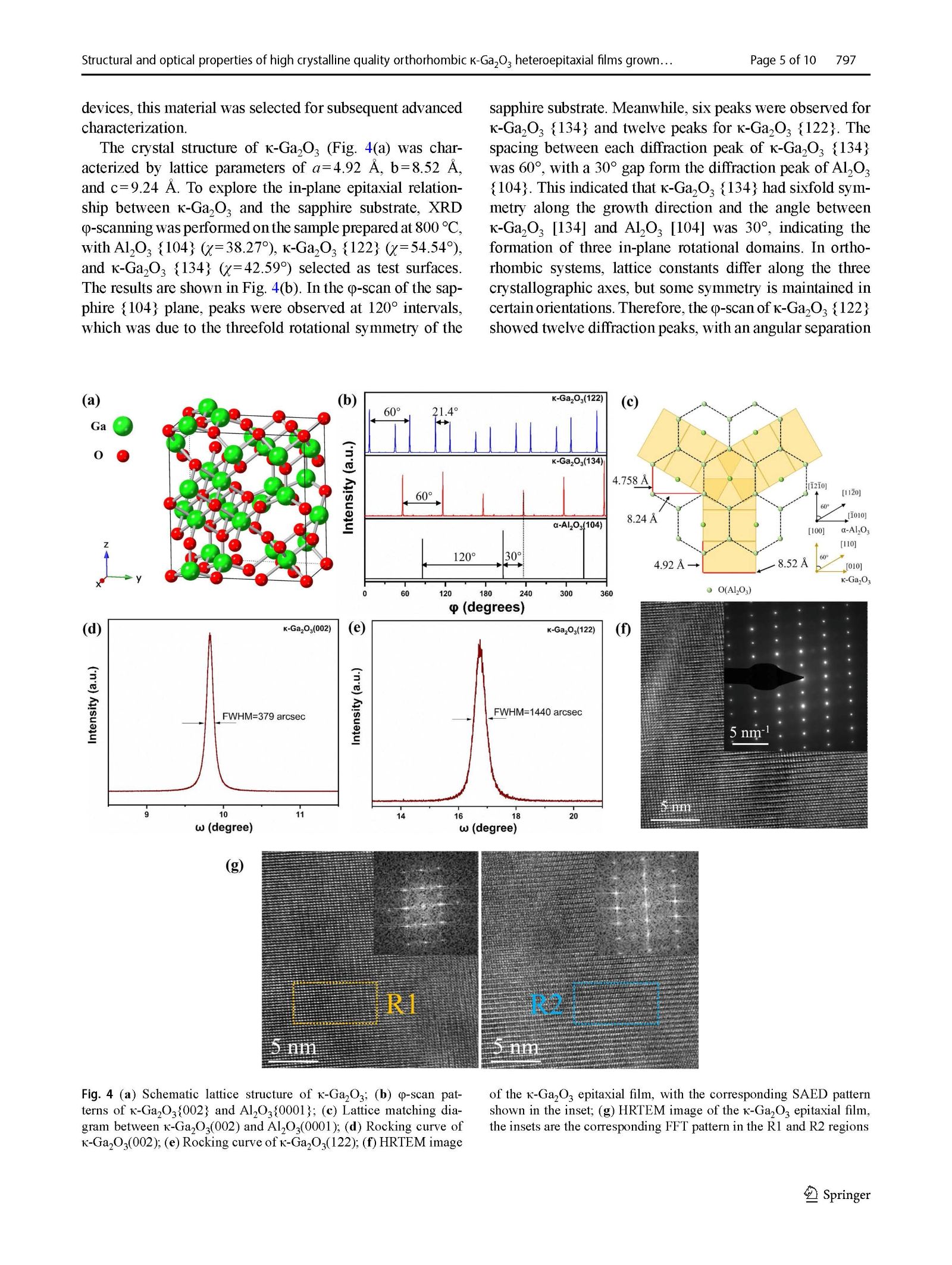
Fig. 4 (a) Schematic lattice structure of κ-Ga2O3; (b) φ-scan patterns of κ-Ga2O3{002} and Al2O3{0001}; (c) Lattice matching diagram between κ-Ga2O3(002) and Al2O3(0001); (d) Rocking curve of κ-Ga2O3(002); (e) Rocking curve of κ-Ga2O3(122); (f) HRTEM image of the κ-Ga2O3 epitaxial film, with the corresponding SAED pattern shown in the inset; (g) HRTEM image of the κ-Ga2O3 epitaxial film, the insets are the corresponding FFT pattern in the R1 and R2 regions.
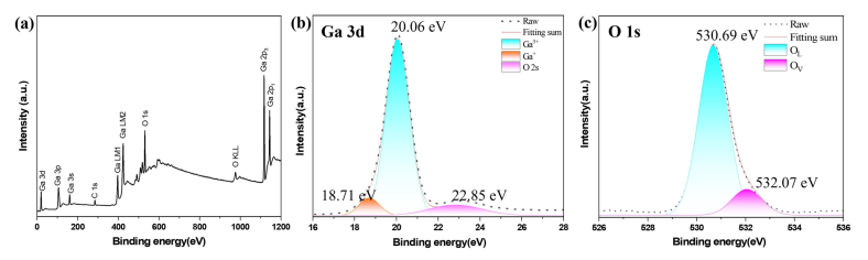
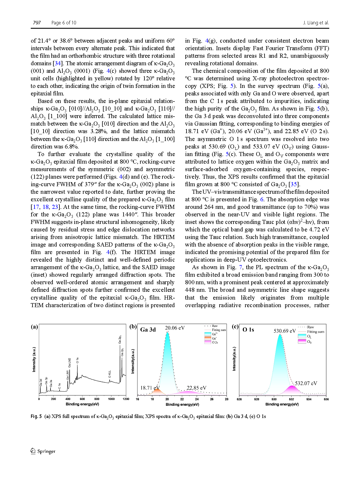
Fig. 5 (a) XPS full spectrum of κ-Ga2O3 epitaxial film; XPS spectra of κ-Ga2O3 epitaxial film: (b) Ga 3 d, (c) O 1s.
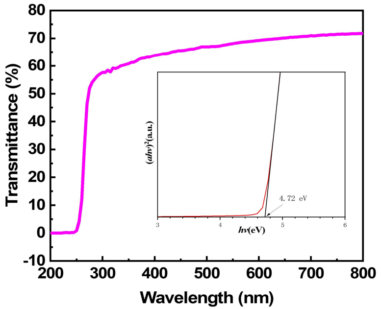
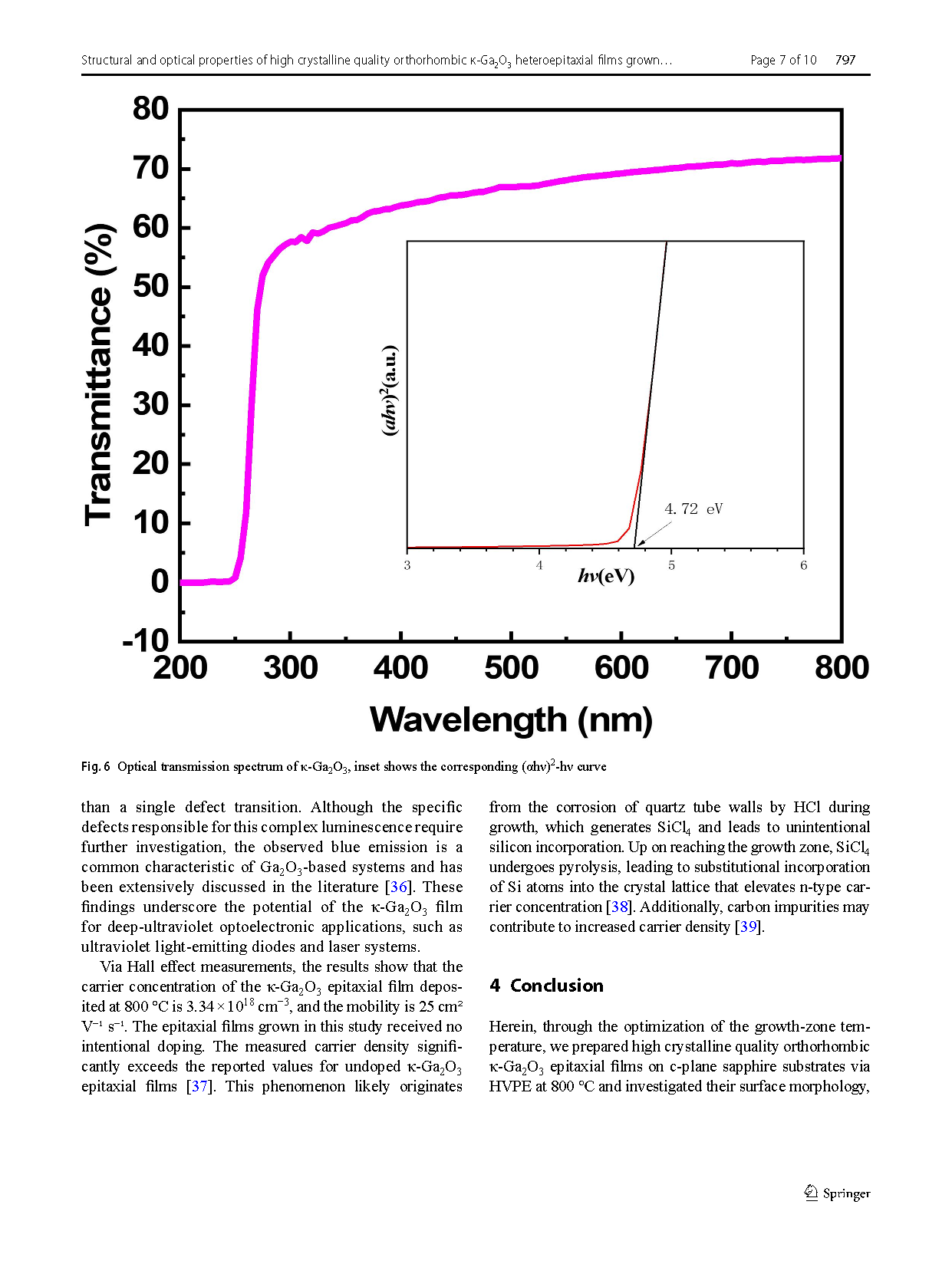
Fig. 6 Optical transmission spectrum of κ-Ga2O3, inset shows the corresponding (αhν)2 -hν curve.
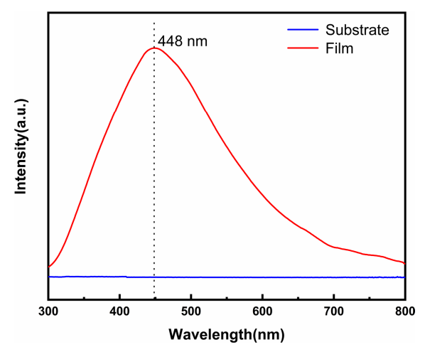
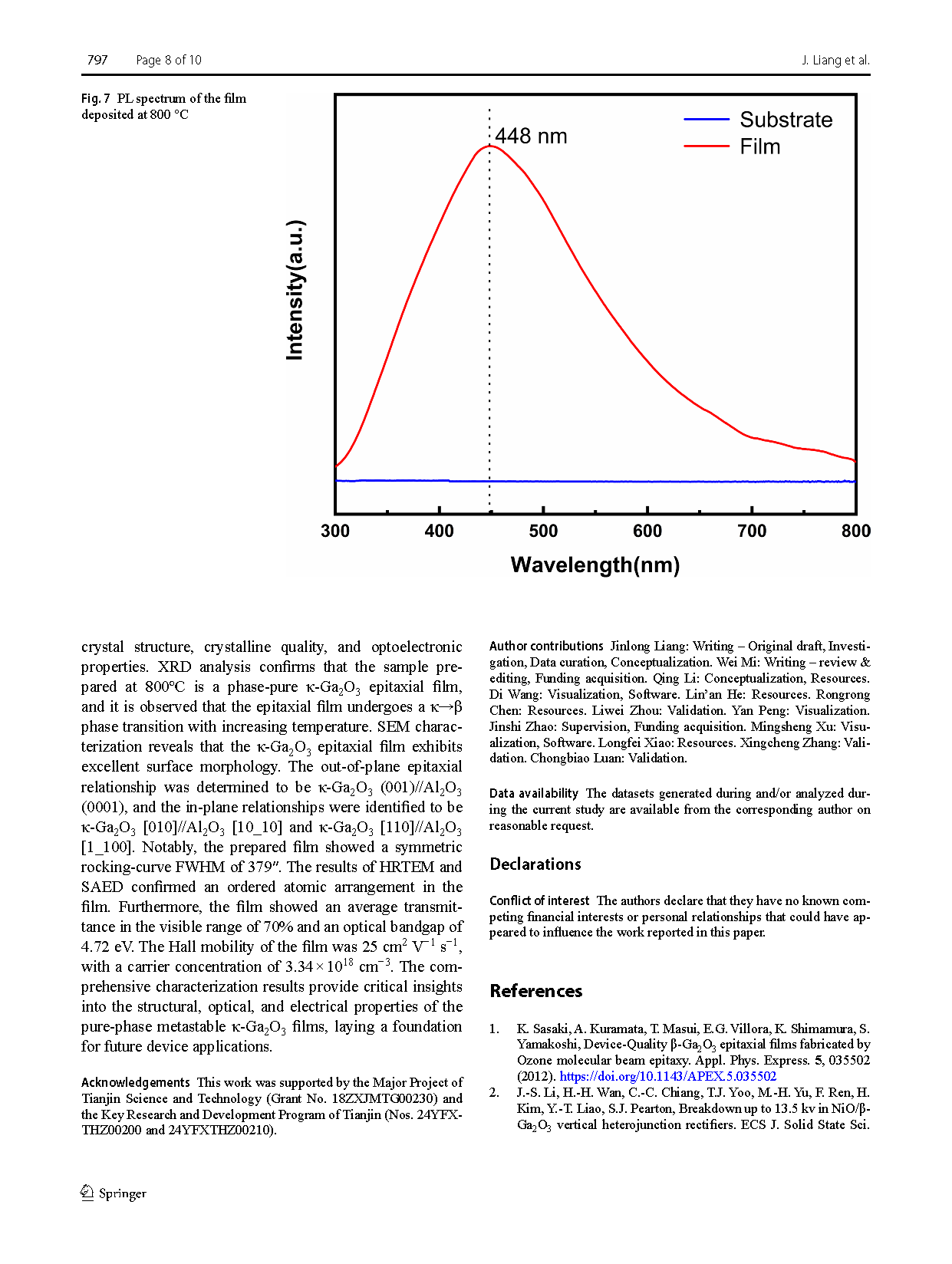
Fig. 7 PL spectrum of the film deposited at 800 °C.
DOI:
doi.org/10.1007/s00339-025-08950-9