Paper Sharing
【Domestic Papers】Growth temperature dependent on the structure, device properties and carrier transport mechanisms of β-Ga₂O₃/GaAs heterojunctions
日期:2025-09-28阅读:595
Researchers from the Shanghai Dianji University have published a dissertation titled "Growth temperature dependent on the structure, device properties and carrier transport mechanisms of β-Ga2O3/GaAs heterojunctions" in Materials Science and Engineering: B.
Project Support
We acknowledge financial support from National Natural Science Foundation of China (U22A2073, 11974433, 91833301).
Background
Solar-blind ultraviolet (UV) photodetectors (PDs) are capable of effectively detecting electromagnetic waves in the 200–280 nm range and play a crucial role in applications such as fire detection, ultraviolet early warning, and deep space exploration. Compared to traditional infrared detectors, solar-blind ultraviolet photodetectors benefit from a natural low-background-noise environment. This advantage arises because stratospheric ozone strongly absorbs solar radiation in the 200–280 nm range. Consequently, these detectors achieve high signal-to-noise ratio (SNR) and low error rates. In recent years, a variety of wide bandgap materials have been used for fabricating solar-blind ultraviolet photodetectors, including AlGaN, ZnMgO and Ga2O3.
Abstract
Ga2O3 features a wide bandgap and excellent optoelectronic properties, making it highly valuable for applications in UV photodetectors, high-power electronics, and transparent conductive materials. Ga2O3 thin films were grown on Si-doped GaAs (100) substrates using pulsed laser deposition technology, followed by the fabrication of Ga2O3/GaAs heterojunction solar-blind ultraviolet detectors. High-quality thin films have been achieved by optimizing the growth temperature. As the growth temperature increased from 500°C to 700°C, the particles deposited on the substrate are provided with sufficient energy to migrate and nucleate, resulting in improved crystallinity and reduced defects in the film. Additionally, the presence of an oxygen atmosphere during deposition reduced the concentration of oxygen vacancies, which further minimized oxygen-vacancy-related defects. As a result, the detector exhibits a 164-fold increase in external quantum efficiency, a 241-fold enhancement in responsivity, and a 44.5 % improvement in Iphoto/Idark. These findings provide an experimental foundation for the development of high-performance β-Ga2O3/GaAs heterojunction solar-blind UV detectors.
Highlights
● Ga2O3/GaAs heterojunctions were fabricated on GaAs via PLD for solar-blind UV detection.
● Optimized growth temperature (500–700 °C) enhanced Ga2O3 crystallinity and reduced defects via improved migration/nucleation.
● Detector achieved 164x EQE, 241x responsivity, 44.5% higher Iphoto/Idark, enabling solar-blind detection.
Conclusion
This work investigates the growth of Ga2O3 thin films on Si-doped (100) GaAs substrates using PLD, particularly on the effect of growth temperature. We have shown that the quality of the films significantly improves when the film deposited at a relatively high temperature. This enhancement can be attributed to the high migration rate of the adsorbed atoms on the substrate surface and the crystallization process, leading to better film crystallization and lower defects. Based on the films, Ga2O3/GaAs heterojunction UV photodetector with a solar-blind response was fabricated. The device fabricated at 700 ◦C exhibited superior performance, with 164-fold and 241-fold enhancements in EQE and responsivity, respectively, and a 44.5 % improvement in Iphoto/Idark compared to devices based on low-quality β-Ga2O3 films. This work provides critical guidance for optimizing β-Ga2O3 deposition and developing high-performance β-Ga2O3/GaAs heterojunction solar-blind UV photodetectors.
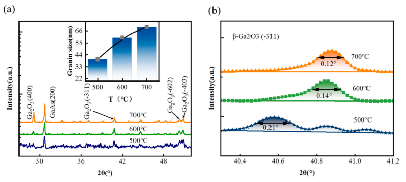
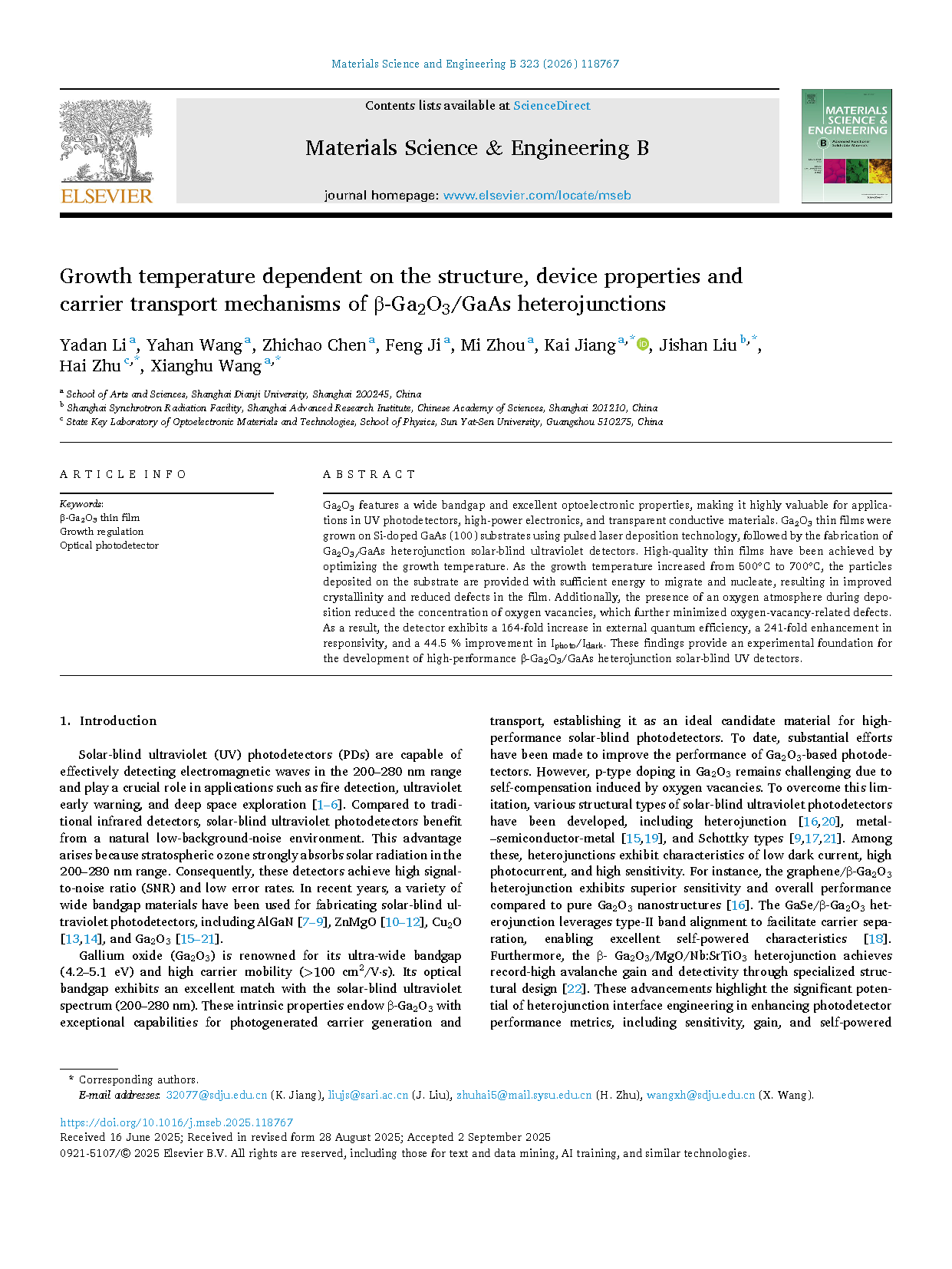
Fig. 1. (a) XRD pattern of the β-Ga2O3 (Inset: Grain size calculated from the (−311) diffraction peak); (b) FWHM comparison of XRD (−311) diffraction peaks for β-Ga2O3.
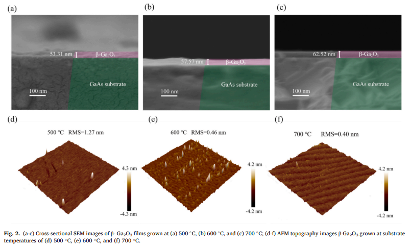
Fig. 2. (a-c) Cross-sectional SEM images of β- Ga2O3 films grown at (a) 500 °C, (b) 600 °C, and (c) 700 °C; (d-f) AFM topography images β-Ga2O3 grown at substrate temperatures of (d) 500 °C, (e) 600 °C, and (f) 700 °C.
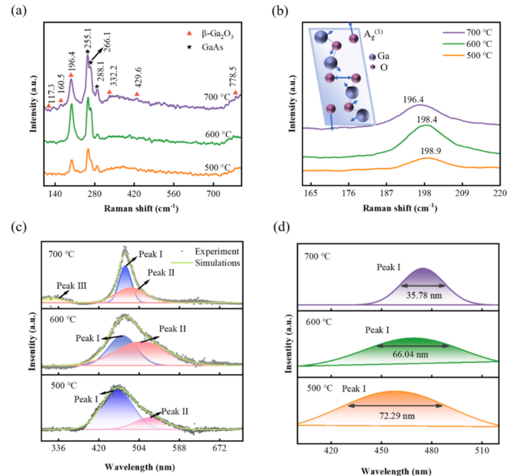
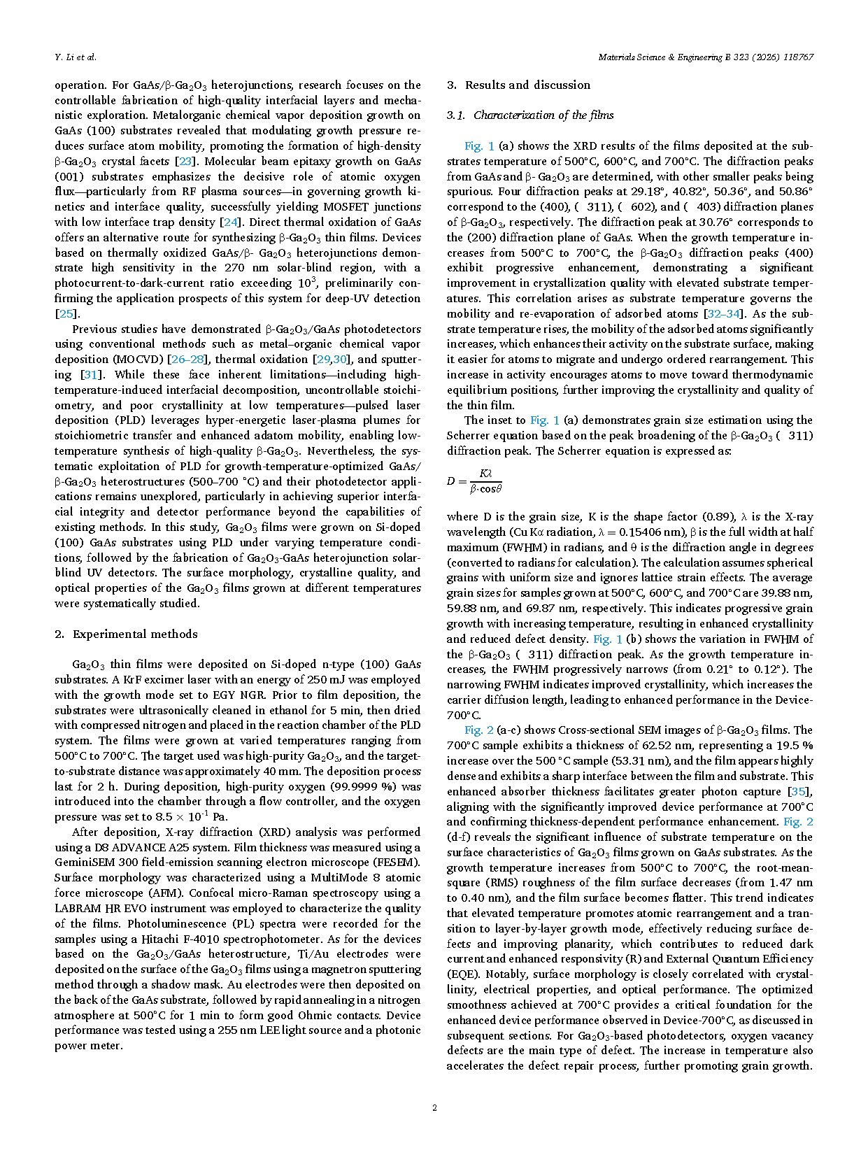
Fig. 3. (a) Raman Spectrum of the β-Ga2O3; (b) Enlarged Raman Spectrum from local region; (c) PL of β-Ga2O3 films; (d) FWHM of Peak I in PL spectra.
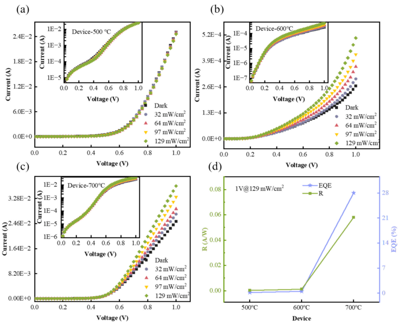
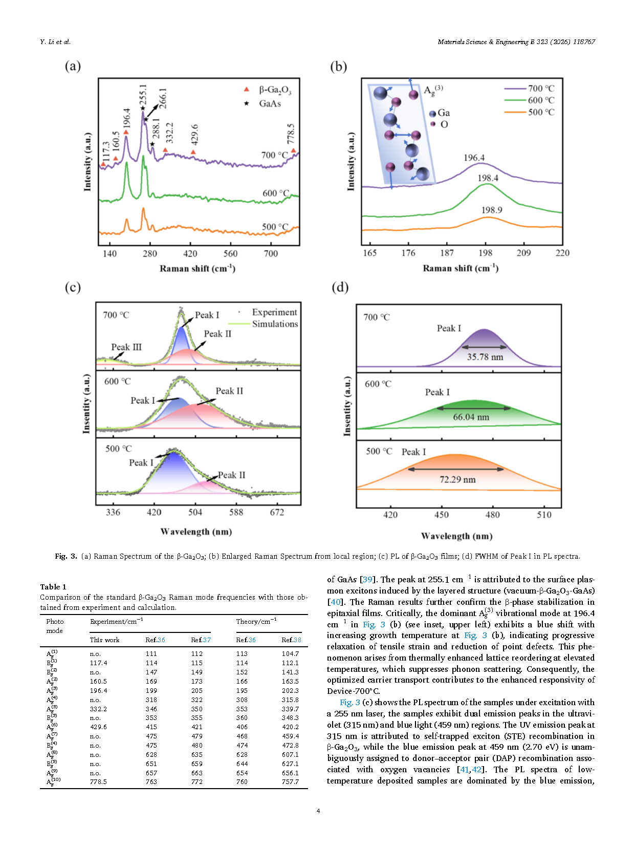
Fig. 4. (a-c) I-V Characteristics (linear scale) of Device-500 °C, 600 °C, and 700 °C (Insets: Logarithmic-scale); (d) Comparison of EQE and R of Device-500 ℃, 600 °C, and 700 °C at 1 V @ 129 mW/cm2.
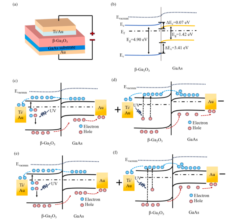
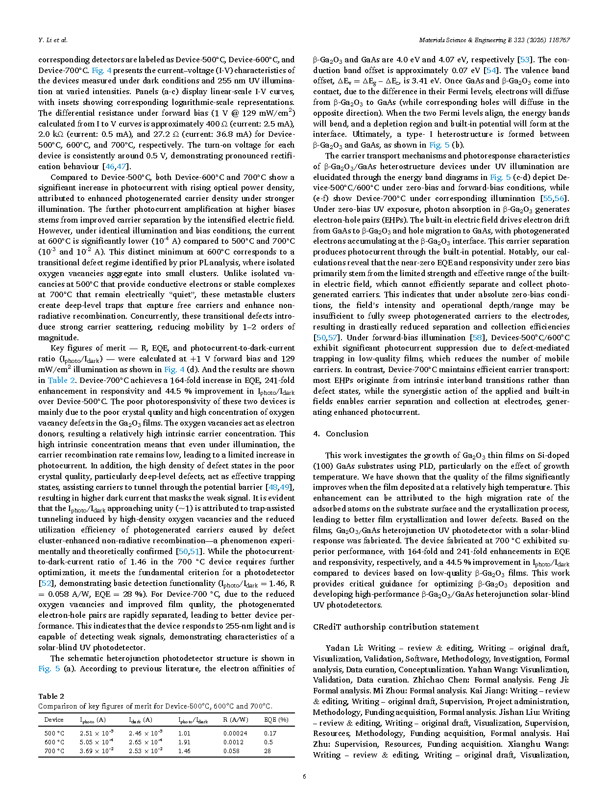
Fig. 5. (a) β-Ga2O3/GaAs heterojunction photodetector structure diagram; (b) The band alignment diagram of β-Ga2O3 and GaAs heterojunction; (c-d) Schematic energy band diagrams of β-Ga2O3/GaAs heterojunction devices (Device-500 ℃ and 600 ℃) under (c) zero-bias and (d) forward-bias UV illumination; (e-f) Corresponding energy band diagrams for Device-700 ℃ under (e) zero-bias and (f) forward-bias UV illumination.
DOI:
doi.org/10.1016/j.mseb.2025.118767