Paper Sharing
【Domestic Papers】Macro-defect-free homoepitaxial (100) β-Ga₂O₃ by MOVPE: Effect of Miscut angles
日期:2025-09-26阅读:519
Researchers from the Sun Yat-Sen University have published a dissertation titled "Macro-defect-free homoepitaxial (100) β-Ga2O3 by MOVPE: Effect of Miscut angles" in Journal of Alloys and Compounds.
Project Support
This work was supported in part by the National Key Research and Development Program of China under Grant 2024YFE0205300; in part by the National Natural Science Foundation of China under Grant 62471504; in part by the Shenzhen institutions of stability support project 20231127114207001; in part by the High-level talent start-up funding project RC2024-008; in part by the Open Fund of the State Key Laboratory of Optoelectronic Materials and Technologies (Sun Yat-sen University) OEMT-2023-KF-05. We sincerely thank Hangzhou Garen Semiconductor Co., Ltd. for providing high-quality Ga2O3 substrates.
Background
β-Ga2O3 with an ultra-wide band gap of ~4.85 eV and a high breakdown electric field of ~8 MV/cm is an emerging candidate for next generation high-power switching devices and radio frequency devices. The Baliga factor of β-Ga2O3 is 4 times of GaN, 10 times of SiC, and 3444 times of Si-based power devices. Moreover, compared to GaN and SiC, bulk β-Ga2O3 single crystals can be prepared using melt growth techniques such as Czochralski method floating zone techniques edge-defined film-fed growth and vertical Bridgman method with significant low cost. Therefore, β-Ga2O3 has attracted more and more attention in both academic and commercial applications.
Abstract
β-Ga2O3 is regarded as an emerging candidate for the next generation of power devices, yet its homoepitaxial growth still needs to be improved. This work aims to provide a deeper understanding of the effect of substrate miscut angles on (100) β-Ga2O3 thick-film homoepitaxy. Homoepitaxial growth of β-Ga2O3 with thickness over 2 μm was investigated via metal-organic vapor phase epitaxy using trimethylgallium as precursor. The growth rate is as high as 0.8 μm/h. Macro-defect-free smooth surface with step flow growth mode was realized on (100) β-Ga2O3 substrates with a miscut angle of 4°. In contrast, epitaxial films on 0°, 1°, and 2° miscut substrates retained macro-defects with the morphology of large mesas and a protrusion grain on the top even after growth condition optimization. Transmission electronic microscopy measurements revealed that the macro-defect with twin region and crystal particle is mainly caused by upward extension of the stacking faults. Increasing the substrate miscut angle can effectively suppress the macro-defects. From the perspective of atomic migration, a large miscut angle with narrow terrace width promotes adatom incorporation at kink sites along atomic steps and effectively reduce the probability of two-dimensional nucleation, thereby preventing the formation of stacking faults and macro-defects. This work demonstrates that large miscut angle is necessary to realize a smooth surface for (100) β-Ga2O3 homoepitaxial films with μm level thickness, which is important for the application of power devices.
Highlights
● Homoepitaxy with micrometer thickness was investigated on (100) β-Ga2O3 substrates.
● The formation of surface macro-defects of the epitaxial films is attributed to the upward extension of the stacking faults.
● The effect of epitaxial mode and substrate miscut angles on the macro-defect formation was investigated.
● A large substrate miscut angle (4°) can suppress two-dimensional nucleation and achieve a macro-defect-free smooth surface during thick-film epitaxy.
Conclusions
In summary, (100) β-Ga2O3 MOCVD homoepitaxy on the substrates with different miscut angles was investigated using TMGa as precursor. The ~2.4 μm thick epitaxial film grown on substrate with a miscut angle of 4° achieved a macro-defect-free smooth surface with the step flow growth mode. In contrast, a lot of surface macro-defects were observed on the epitaxial films grown on the substrates with small miscut angles even after the optimization of the growth mode. TEM images reveal the surface macro-defects are crystal particles and mainly caused by the upward extension of the stacking faults. For small miscut angles, the kink points of the atomic steps are insufficient, and some of the adsorb atoms are likely to form kink sites by two-dimensional nucleation, resulting in the stacking faults and surface macro-defects in the further homoepitaxy process. As the miscut angle increases, the number of kink sites increases significantly, and the probability of two-dimensional nucleation is reduced. As a result, a smooth and macro-defect-free surface for homoepitaxial thick film was achieved by suppressing the stacking faults. Our work provides a deeper understanding of (100) β-Ga2O3 homoepitaxy and foundation for power device applications.
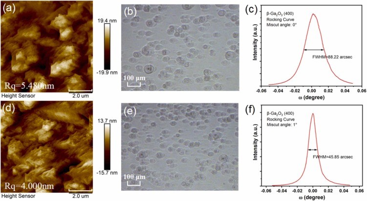
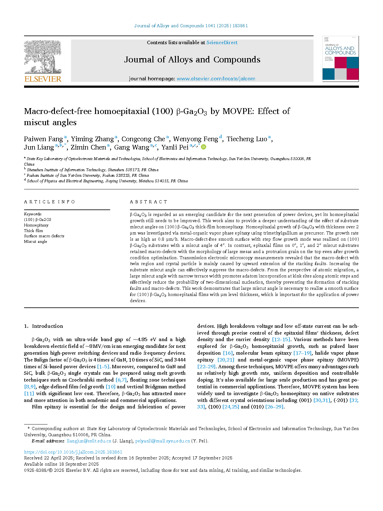
Fig. 1. The AFM images with 8 μm range, optical microscope images and HRXRD rocking curves of the homoepitaxial films grown on (100) β-Ga2O3 substrates with miscut angles of (a) (b) (c) 0° and (d) (e) (f) 1°.
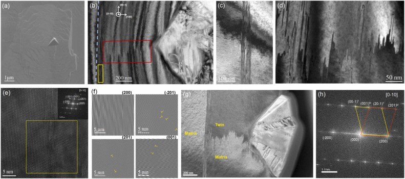
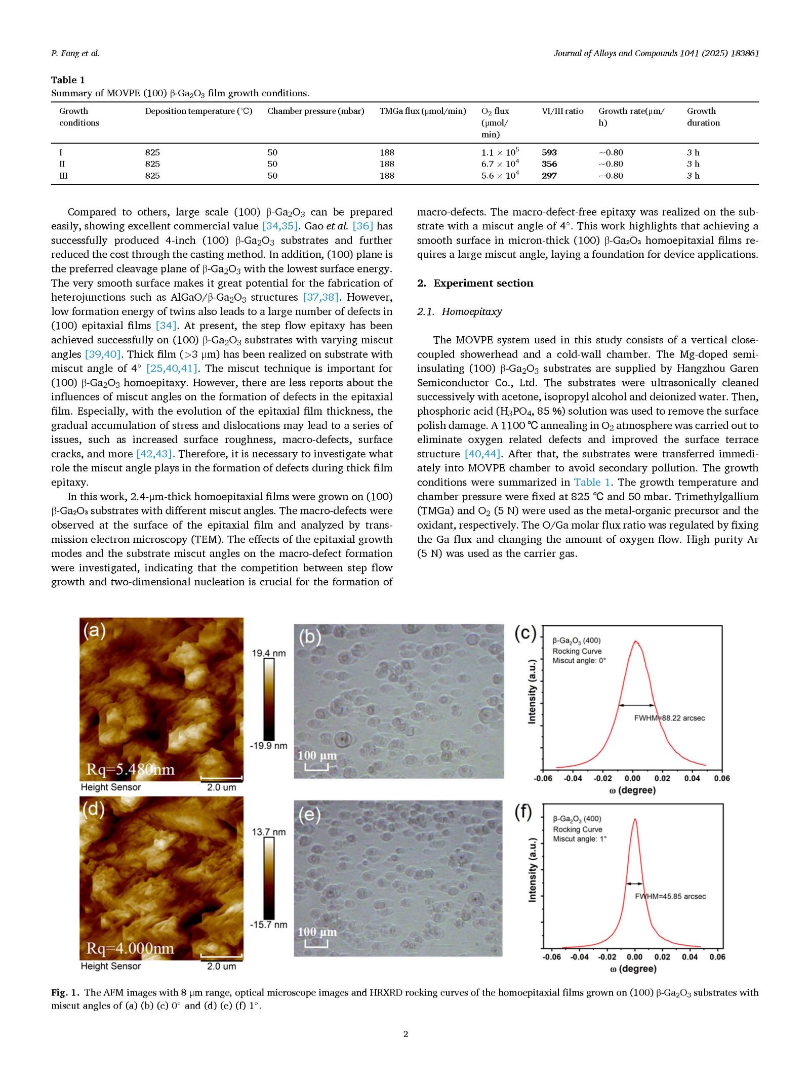
Fig. 2. (a) The SEM image of the surface macro defect; (b) the cross sectional TEM image of the macro-defect for the sample without miscut angle; (c) and (d) are the enlarged images of the yellow frame and the red frame in (b), respectively; (e) The HRTEM pattern of the stacking faults (the inset corresponds to the FFT image of the yellow framed area); (f) the IFFT images of the yellow framed area in (e); (g) and (h) are the bright field image and its corresponded FFT image.
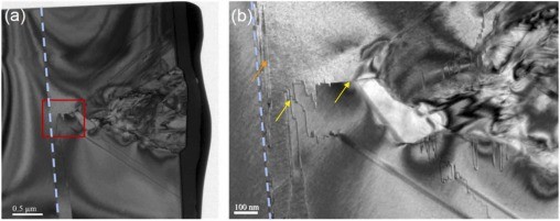
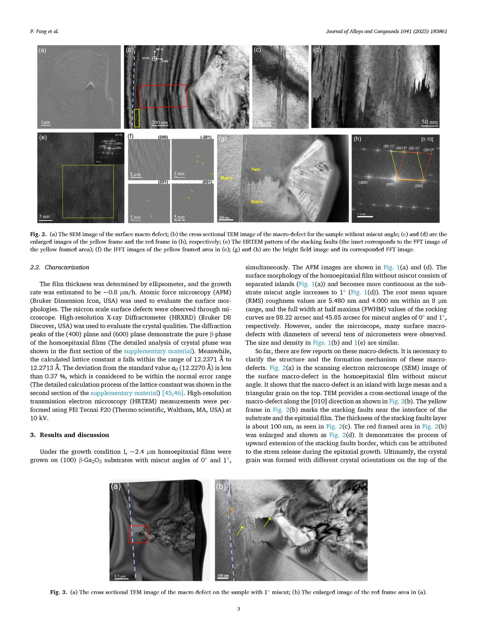
Fig. 3. (a) The cross sectional TEM image of the macro defect on the sample with 1° miscut; (b) The enlarged image of the red frame area in (a).
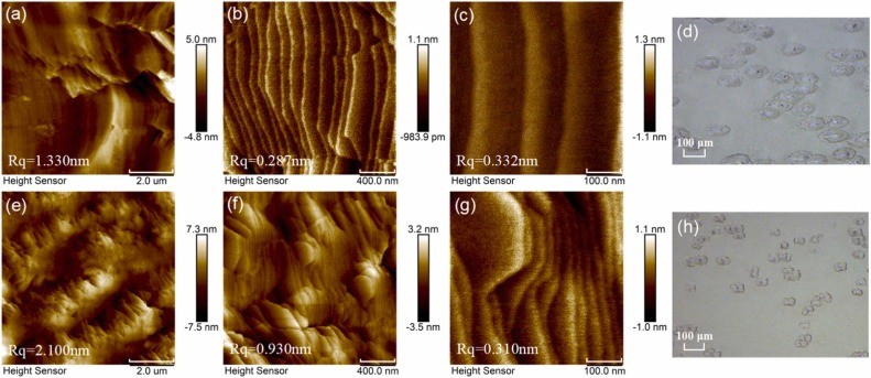
Fig. 4. The AFM images within the (a) 8 μm, (b) 2 μm and (c) 0.5 μm ranges and (d) the optical microscope images of the β-Ga2O3 film grown on the (100) β-Ga2O3 substrate without miscut angle at growth condition II. The AFM images within the (e) 8 μm, (f) 2 μm and (g) 0.5 μm ranges and (h) the optical microscope image of the β-Ga2O3 film grown on the (100) β-Ga2O3 substrate with a miscut angle of 1° at growth condition III.
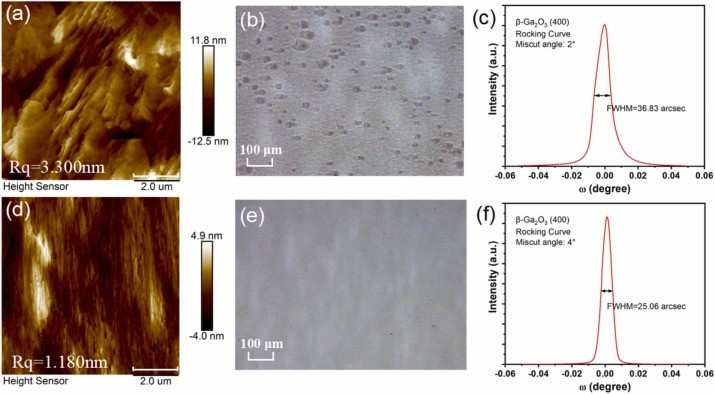
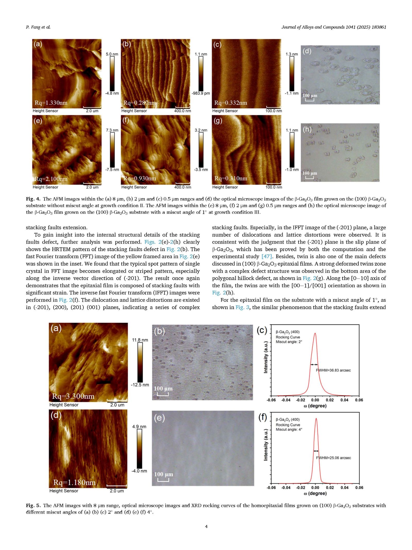
Fig. 5. The AFM images with 8 μm range, optical microscope images and XRD rocking curves of the homoepitaxial films grown on (100) β-Ga2O3 substrates with different miscut angles of (a) (b) (c) 2° and (d) (e) (f) 4°.
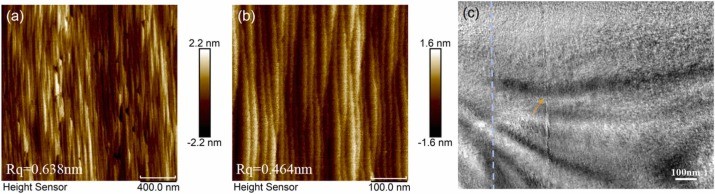
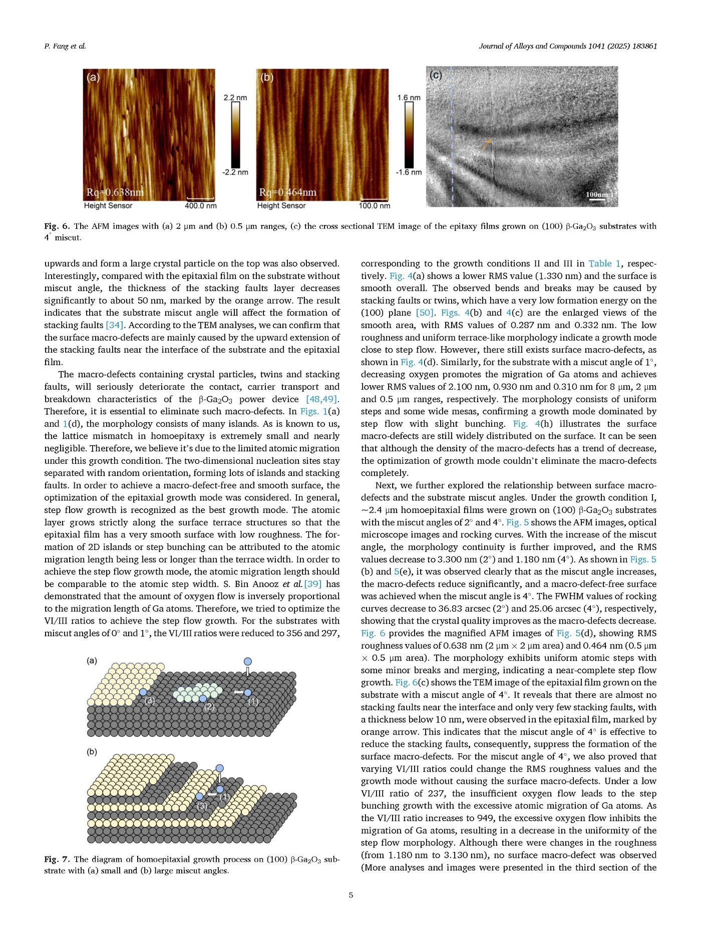
Fig. 6. The AFM images with (a) 2 μm and (b) 0.5 μm ranges, (c) the cross sectional TEM image of the epitaxy films grown on (100) β-Ga2O3 substrates with 4° miscut.
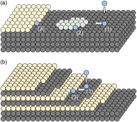
Fig. 7. The diagram of homoepitaxial growth process on (100) β-Ga2O3 substrate with (a) small and (b) large miscut angles.
DOI:
doi.org/10.1016/j.jallcom.2025.183861