Paper Sharing
【Member Papers】A novel single event effect radiation hardening design in β-Ga₂O₃ Schottky barrier diodes
日期:2025-09-24阅读:468
Researchers from the Sichuan University have published a dissertation titled "A novel single event effect radiation hardening design in β-Ga2O3 Schottky barrier diodes" in Nuclear Instruments and Methods in Physics Research Section B: Beam Interactions with Materials and Atoms.
Project Support
This project is supported by the Sichuan University-Suining City Strategic Cooperation Technology Projects under Grant No. 2023CDSN-11.
Background
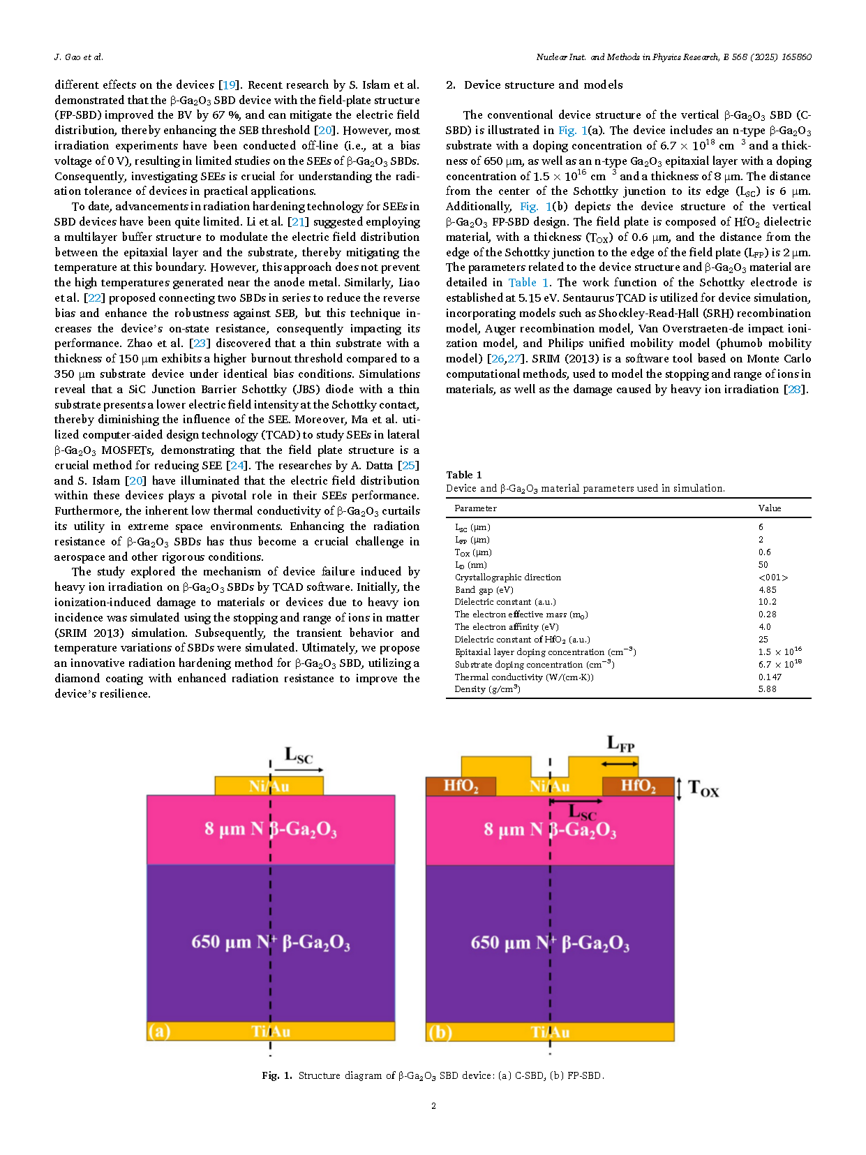
β-Ga2O3 is an ultra-wide band gap semiconductor material with a band gap of 4.6 eV to 4.9 eV, a theoretical critical breakdown field strength exceeding 8 MV/cm, and a high Baliga figure of merit (BFOM), making it a promising material for high-power electronics, radio frequency applications, and aerospace fields. Representative devices based on β-Ga2O3 include metal-oxide semiconductor field effect transistors (MOS) and Schottky barrier diodes (SBDs). So far, the rapid development of β-Ga2O3 materials has led to reports of high reverse breakdown voltage (BV) and high BFOM in related power devices. The radiation resistance of semiconductor devices is of vital importance to their manufacturing and application. Typical irradiation effects, such as total ionizing dose (TID) and single event effect (SEE), can reduce the electrical performance of devices, induce deep defects, and even lead to complete failure. The inherent low thermal conductivity of β-Ga2O3 material makes it difficult for the local heat generated when bombarded by particles to dissipate quickly, causing a sharp increase in lattice temperature and intensifying the risk of single event burnout (SEB). The traditional anti-radiation reinforcement technology is mainly used to regulate the distribution of the electric field, but its effect on solving the problem of heat accumulation is limited. Therefore, there is an urgent need for a comprehensive reinforcement design that can simultaneously address the issues of electric field and heat.
Abstract
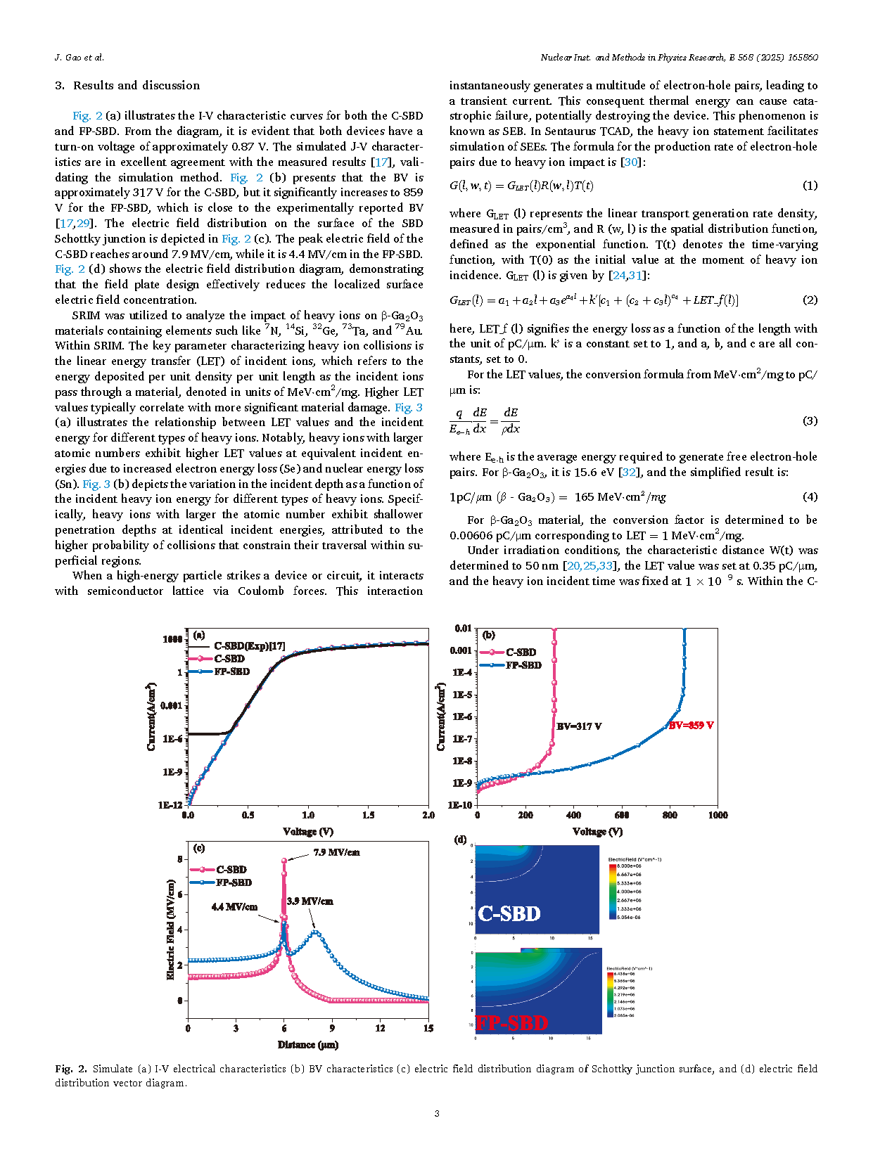
The single event effects (SEEs) of the four types of β-Ga2O3 Schottky barrier diode (SBD) device structures were simulated using Sentaurus TCAD. The analysis reveals that the variations in bias voltage (VR) and linear energy transfer (LET) have a significant impact on these effects. The simulations highlight that both the distribution of the electric field and the peak lattice temperature (TMax) within the device are key determinants of SEEs in β-Ga2O3 SBDs. The results indicate that the breakdown voltage (BV) of the β-Ga2O3 SBD integrated with a field plate terminal technique (FP-SBD) is enhanced by approximately 170.9 % compared to the conventional device structure without the field plate terminal (C-SBD). Compared to the FP-SBD, the FP-SBD with diamond coating (FP-SBD-D) exhibits approximately 26.3 % reduction in the peak transient current and 40.3 % reduction in TMax, effectively tackling the aforementioned issues effectively. Subsequently, a notable decline in the internal collision ionization rate and current density is observed after exposure to heavy ion impacts. This study demonstrates that the synergistic effect of the FP-SBD-D effectively alleviates the influence of SEEs on β-Ga2O3 SBDs, thereby diminishing the likelihood of single event burnout (SEB) in the device.
Conclusion
The novel strategy is proposed to tackle the thermal conductivity challenge in β-Ga2O3 SBDs using integrating field plate terminal technology with diamond coating induced by SEEs. The research findings reveal an increase in both the maximum transient current and Tmax values with higher VR and LET values. Furthermore, the interplay of the electric field distribution and lattice temperature within the device is a critical factor in determining the occurrence of SEB. TCAD simulations show that FP-SBD can alleviate the electric field distribution and enhance the BV of the C-SBD by 170.9 %. Compared to the FP-SBD, the FP-SBD-D exhibits a reduction of approximately 26.3 % in peak transient current and 40.3 % in TMax under the conditions of VR = 100 V and LET = 0.35 pC/μm. This approach effectively lowers the internal collision ionization rate and current density, thereby reducing the impact of SEEs on device performance and minimizing the risk of SEB. The proposed hardening technique offers a novel strategy for enhancing the radiation tolerance of β-Ga2O3 SBDs.
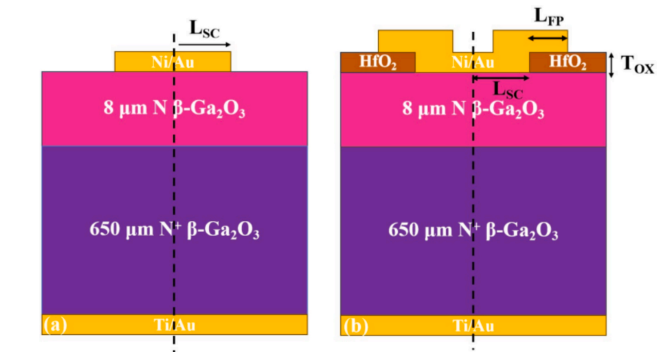
Fig. 1. Structure diagram of β-Ga2O3 SBD device: (a) C-SBD, (b) FP-SBD.
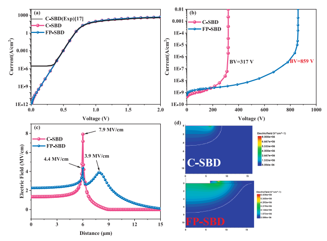
Fig. 2. Simulate (a) I-V electrical characteristics (b) BV characteristics (c) electric field distribution diagram of Schottky junction surface, and (d) electric field distribution vector diagram.
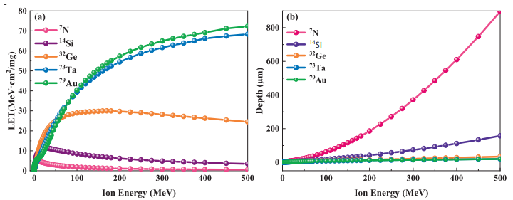
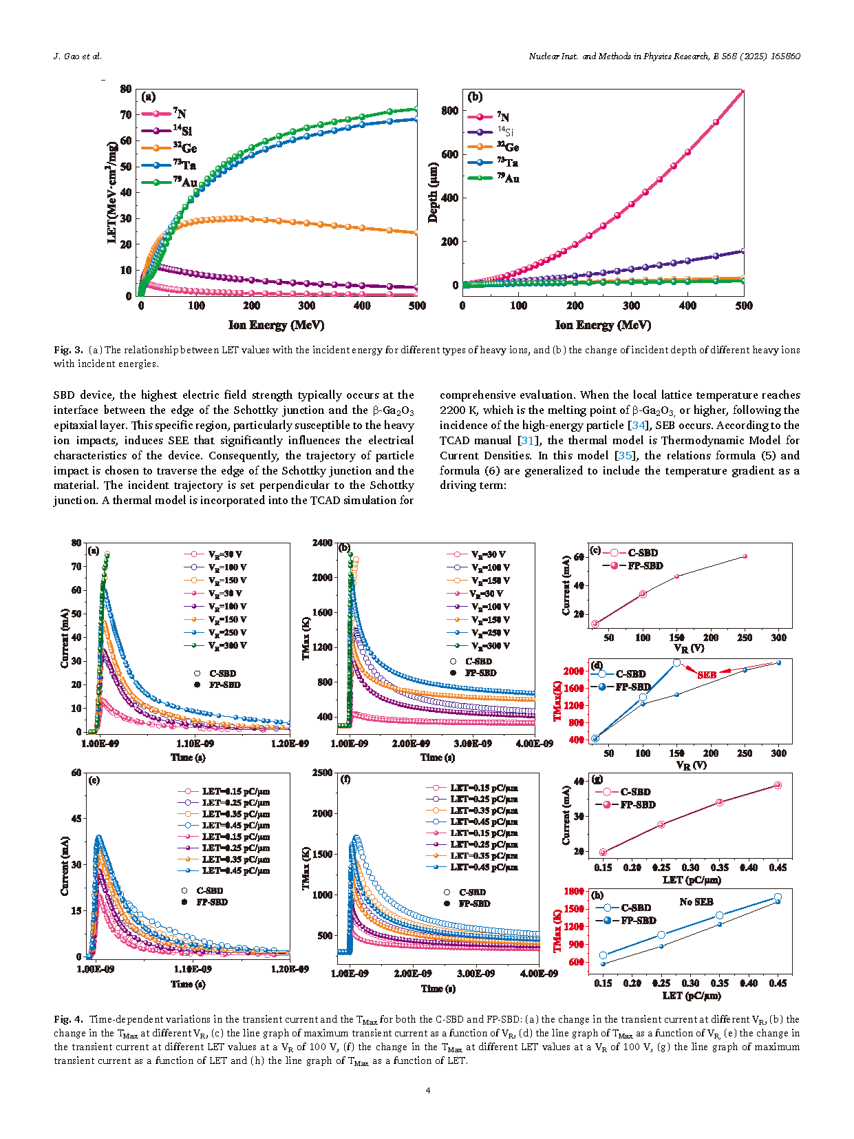
Fig. 3. (a) The relationship between LET values with the incident energy for different types of heavy ions, and (b) the change of incident depth of different heavy ions with incident energies.
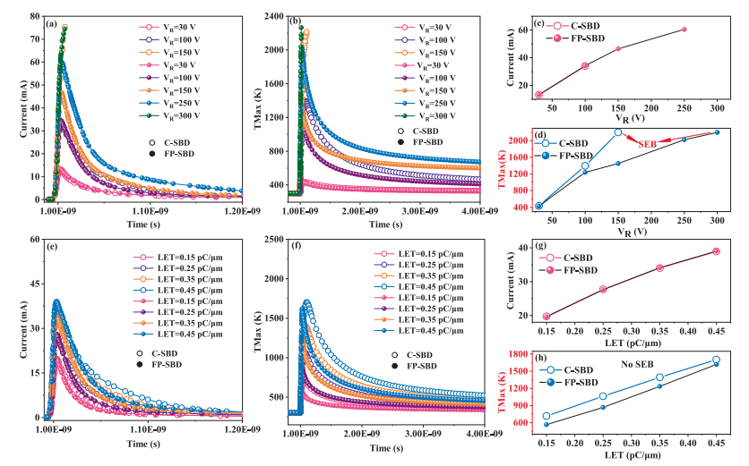
Fig. 4. Time-dependent variations in the transient current and the TMax for both the C-SBD and FP-SBD: (a) the change in the transient current at different VR, (b) the change in the TMax at different VR, (c) the line graph of maximum transient current as a function of VR, (d) the line graph of TMax as a function of VR, (e) the change in the transient current at different LET values at a VR of 100 V, (f) the change in the TMax at different LET values at a VR of 100 V, (g) the line graph of maximum transient current as a function of LET and (h) the line graph of TMax as a function of LET.
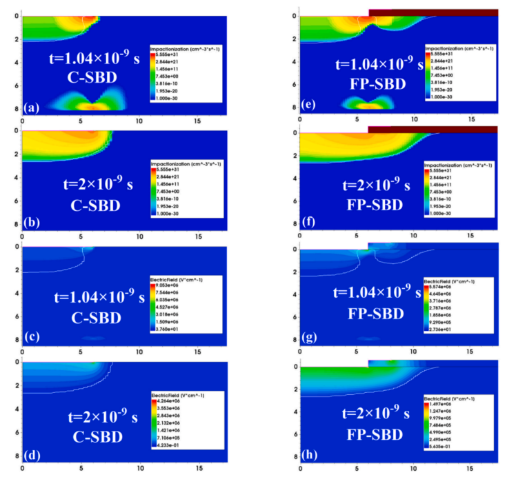
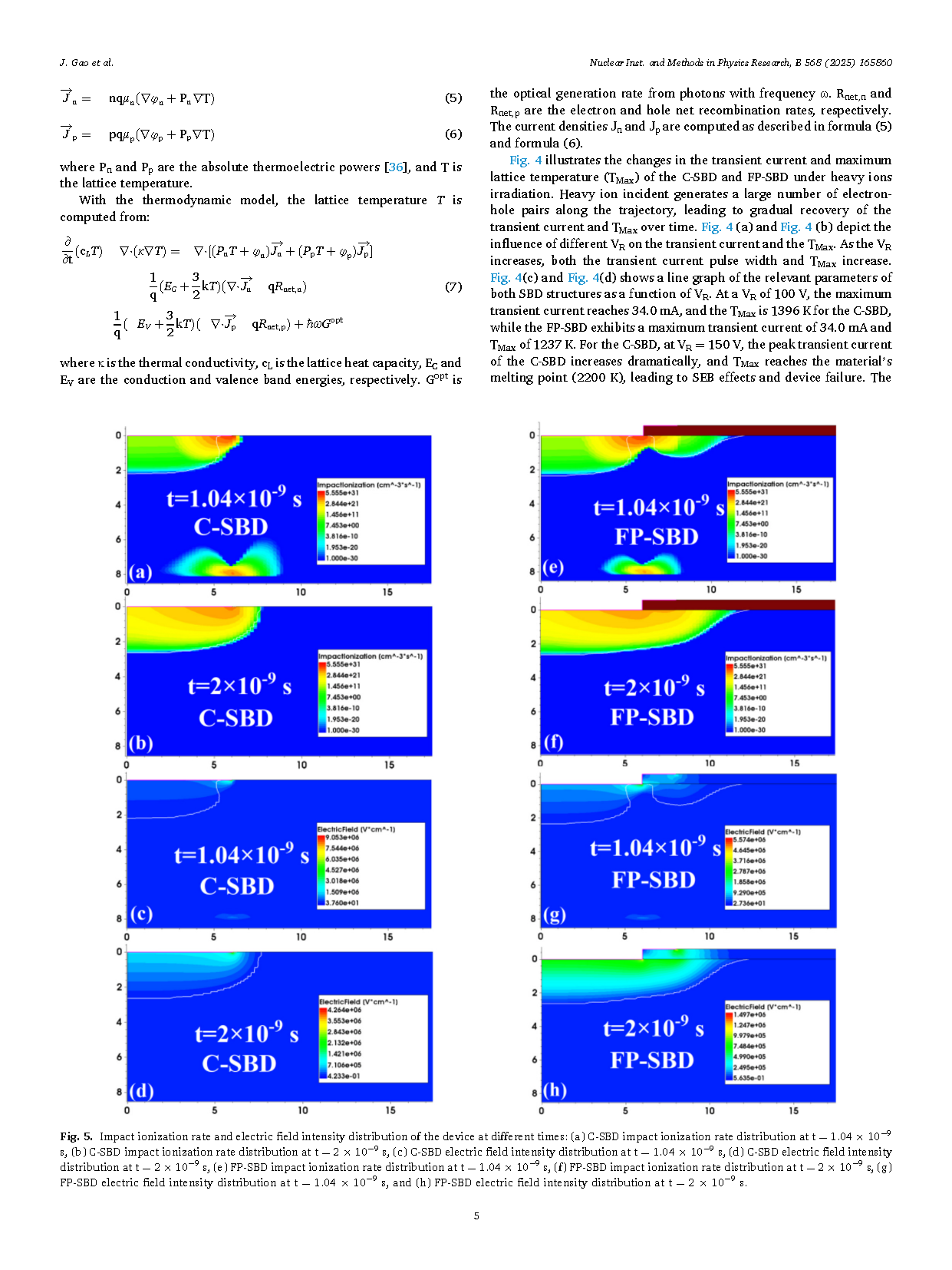
Fig. 5. Impact ionization rate and electric field intensity distribution of the device at different times: (a) C-SBD impact ionization rate distribution at t = 1.04 × 10⁻⁹ s, (b) C-SBD impact ionization rate distribution at t = 2 × 10⁻⁹ s, (c) C-SBD electric field intensity distribution at t = 1.04 × 10⁻⁹ s, (d) C-SBD electric field intensity distribution at t = 2 × 10⁻⁹ s, (e) FP-SBD impact ionization rate distribution at t = 1.04 × 10⁻⁹ s, (f) FP-SBD impact ionization rate distribution at t = 2 × 10⁻⁹ s, (g) FP-SBD electric field intensity distribution at t = 1.04 × 10⁻⁹ s, and (h) FP-SBD electric field intensity distribution at t = 2 × 10⁻⁹ s.
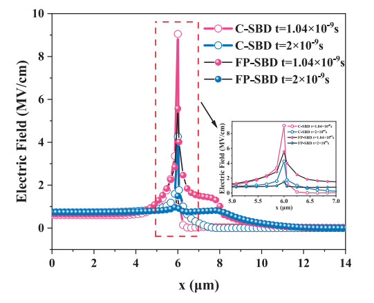
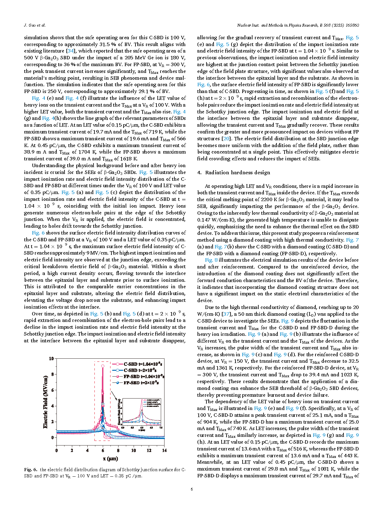
Fig. 6. the electric field distribution diagram of Schottky junction surface for C-SBD and FP-SBD at VR = 100 V and LET = 0.35 pC /μm.
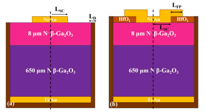
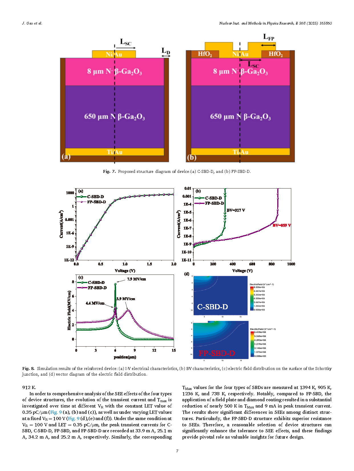
Fig. 7. Proposed structure diagram of device:(a) C-SBD-D, and (b) FP-SBD-D.
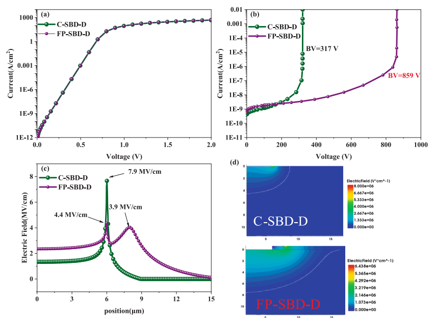
Fig. 8. Simulation results of the reinforced device: (a) I-V electrical characteristics, (b) BV characteristics, (c) electric field distribution on the surface of the Schottky junction, and (d) vector diagram of the electric field distribution.
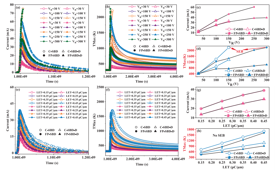
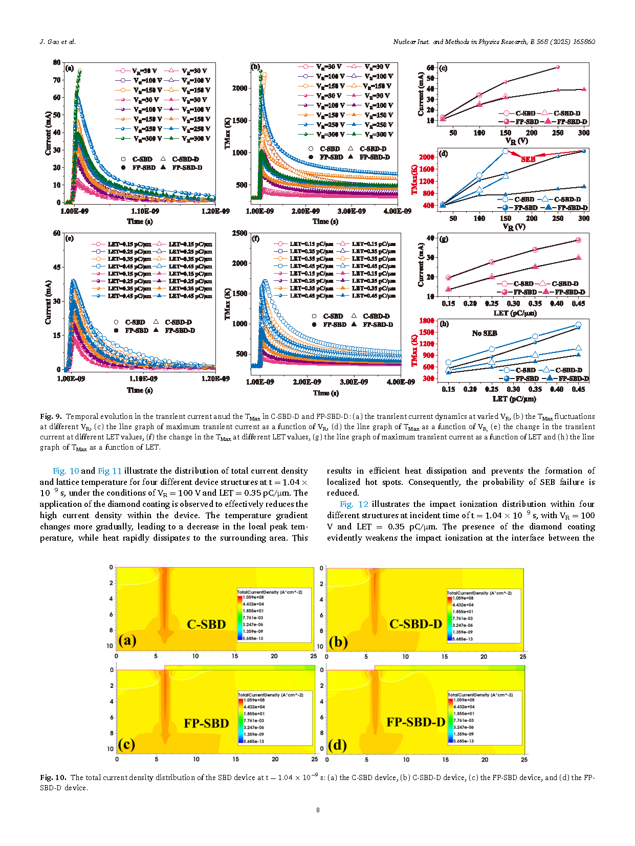
Fig. 9. Temporal evolution in the transient current and the TMax in C-SBD-D and FP-SBD-D: (a) the transient current dynamics at varied VR, (b) the TMax fluctuations at different VR, (c) the line graph of maximum transient current as a function of VR, (d) the line graph of TMax as a function of VR, (e) the change in the transient current at different LET values, (f) the change in the TMax at different LET values, (g) the line graph of maximum transient current as a function of LET and (h) the line graph of TMax as a function of LET.
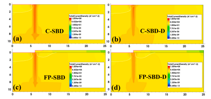
Fig. 10. The total current density distribution of the SBD device at t = 1.04 × 10⁻⁹ s: (a) the C-SBD device, (b) C-SBD-D device, (c) the FP-SBD device, and (d) the FP-SBD-D device.
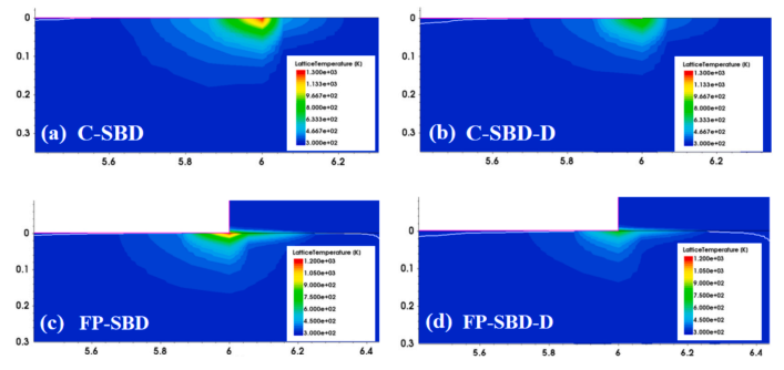
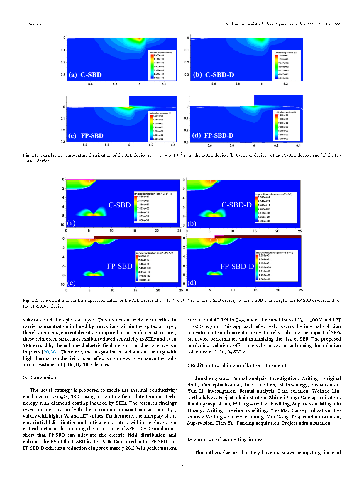
Fig. 11. Peak lattice temperature distribution of the SBD device at t = 1.04 × 10⁻⁹ s: (a) the C-SBD device, (b) C-SBD-D device, (c) the FP-SBD device, and (d) the FPSBD-D device.
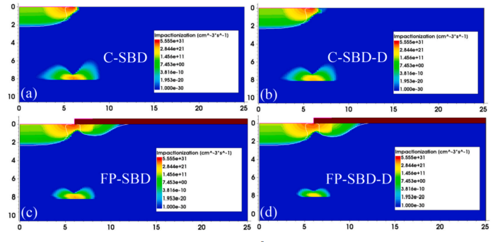
Fig. 12. The distribution of the impact ionization of the SBD device at t = 1.04 × 10⁻⁹ s: (a) the C-SBD device, (b) the C-SBD-D device, (c) the FP-SBD device, and (d) the FP-SBD-D device.
DOI:
doi.org/10.1016/j.nimb.2025.165860