


Paper Sharing
【Member Papers】Sn doping induced interfacial barrier height tailoring in Ga₂O₃ deep-ultraviolet photodetector
日期:2025-09-23阅读:469
One of the charms of semiconductors is that device performance can be optimized through adjustable elemental doping. Compared with heavy doping, light doping is more efficient and sufficient to achieve fine material property regulation and band structure trimming.
Recently, Professor Tang Weihua from Nanjing University of Posts and Telecommunications, Professor Liu Zeng from Inner Mongolia University, and Dr. Zhang Zhang from Nanjing University of Science and Technology, among others, published a paper in Science China Materials, using a simple plasma-enhanced chemical vapor phase technique. A series of tin-doped Gallium Oxide films (Sn:Ga=0-1.14 at.%) were prepared.
Key Points
1) With the change of oxygen vacancy (OⅡ) concentration, both the film conductivity and the atypical Schottky junction behavior at the Ti/Sn-GaO3 interface can be adjusted. The two jointly affect the carrier transport process and the corresponding detection performance within the Au/Ti/Sn-Ga2O3/Ti/Au photodetector.
2) When the OⅡ concentration rises to 38.88%, the interface Schottky barrier height drops to 0.54 eV, which is conducive to electron tunneling and enables the device response to reach an excellent level of 1880 mA/W.
3) Conversely, when the OⅡ concentration is reducedⅡ to 30%, the barrier height increases to 0.70 eV, effectively suppressing the dark current (28.4 pA) while enhancing the device's specific detection rate (1.44×10¹³ Jones) and the light-dark current ratio (3.42×10⁴).
This study highlights the importance of balancing doping concentration with performance optimization and reveals the significant potential of interface engineering for regulating the electron transport behavior and performance of semiconductor devices.
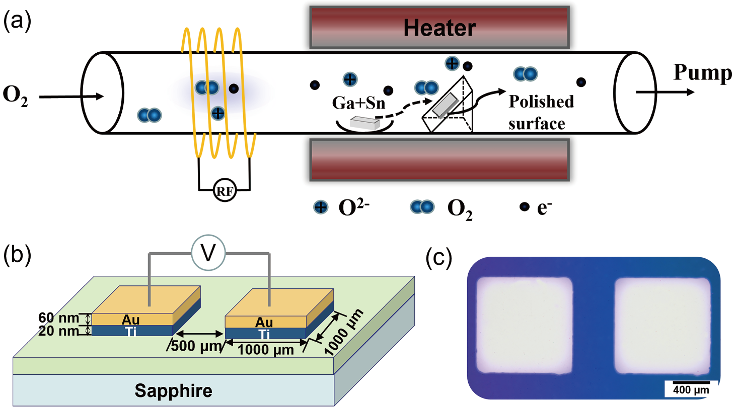
Figure 1. (a) Schematic diagram of the PECVD system. (b) Structure diagram and (c) top-view microscopy image of the fabricated Sn-doped Ga2O3 film-based PD.
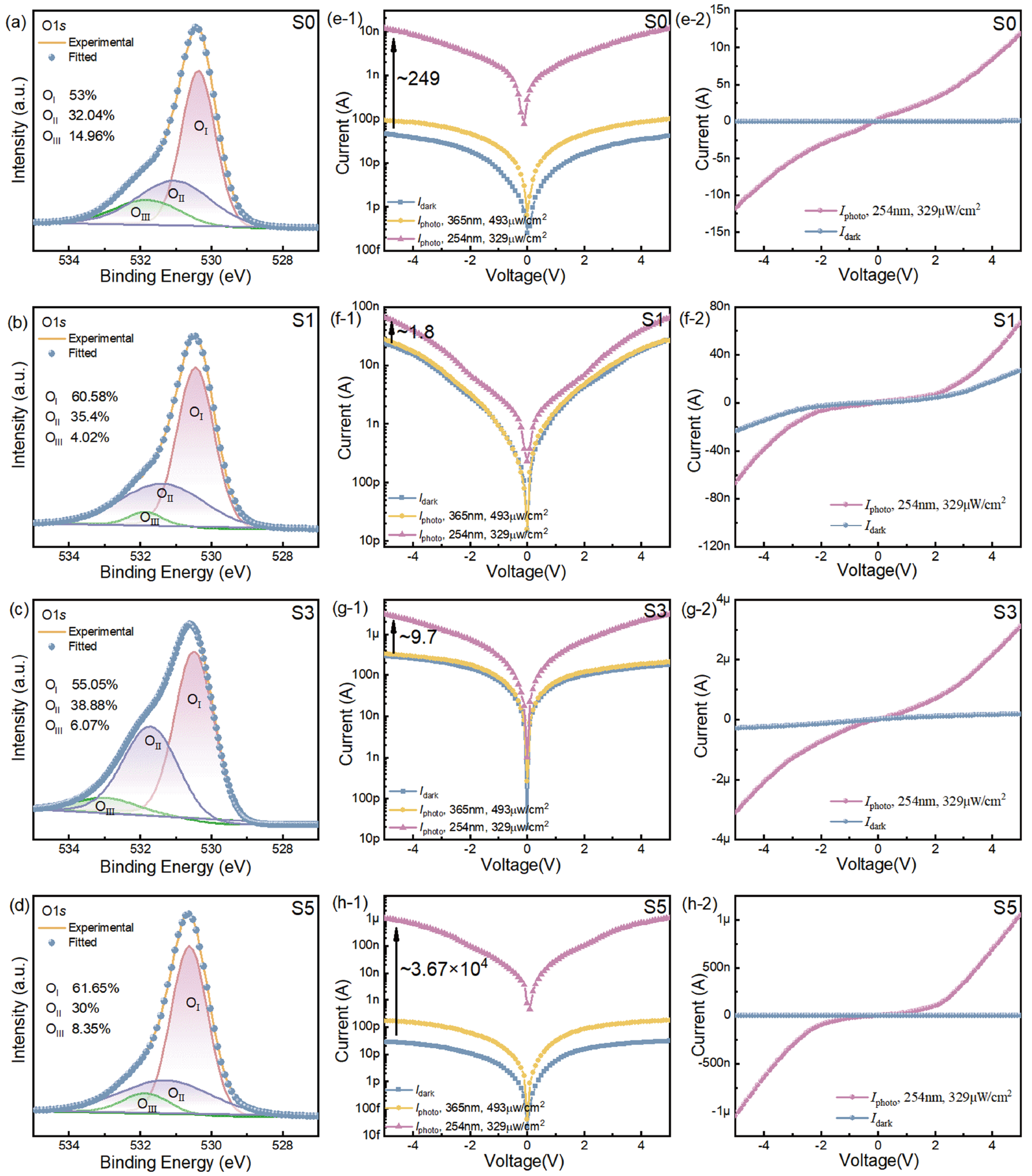
Figure 2. O 1s high-resolution XPS spectra of (a) S0, (b) S1, (c) S3, and (d) S5 samples. The log-scale (1) and linear (2) I-V characteristics of the corresponding (e) S0, (f) S1, (g) S3, and (h) S5 devices under dark conditions and light illumination.
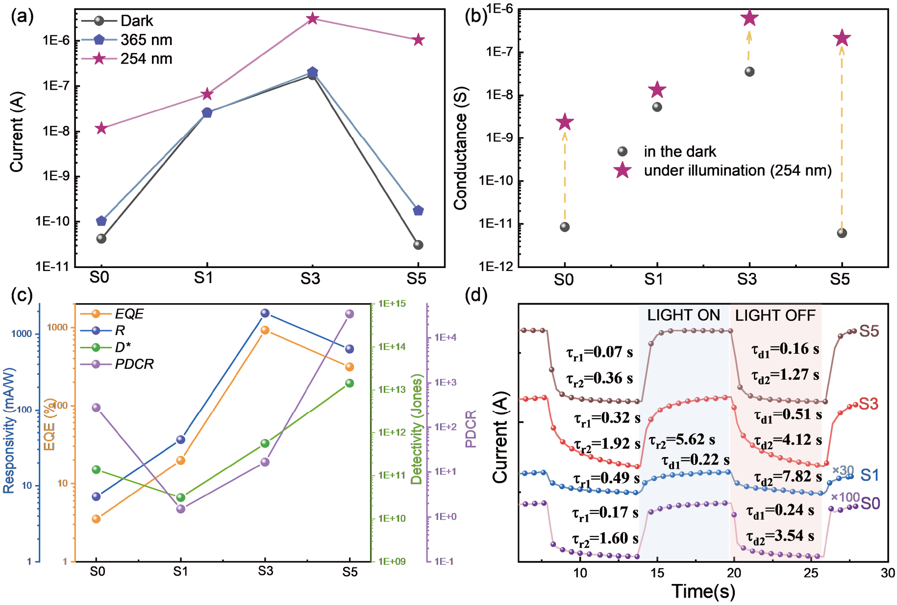
Figure 3. (a) Current and (b) conductance comparison of S0–S5 devices under dark conditions and light illumination. (c) EQE, R, D*, and PDCR comparison of S0–S5 devices. (d) I-t curves of S0–S5 devices.
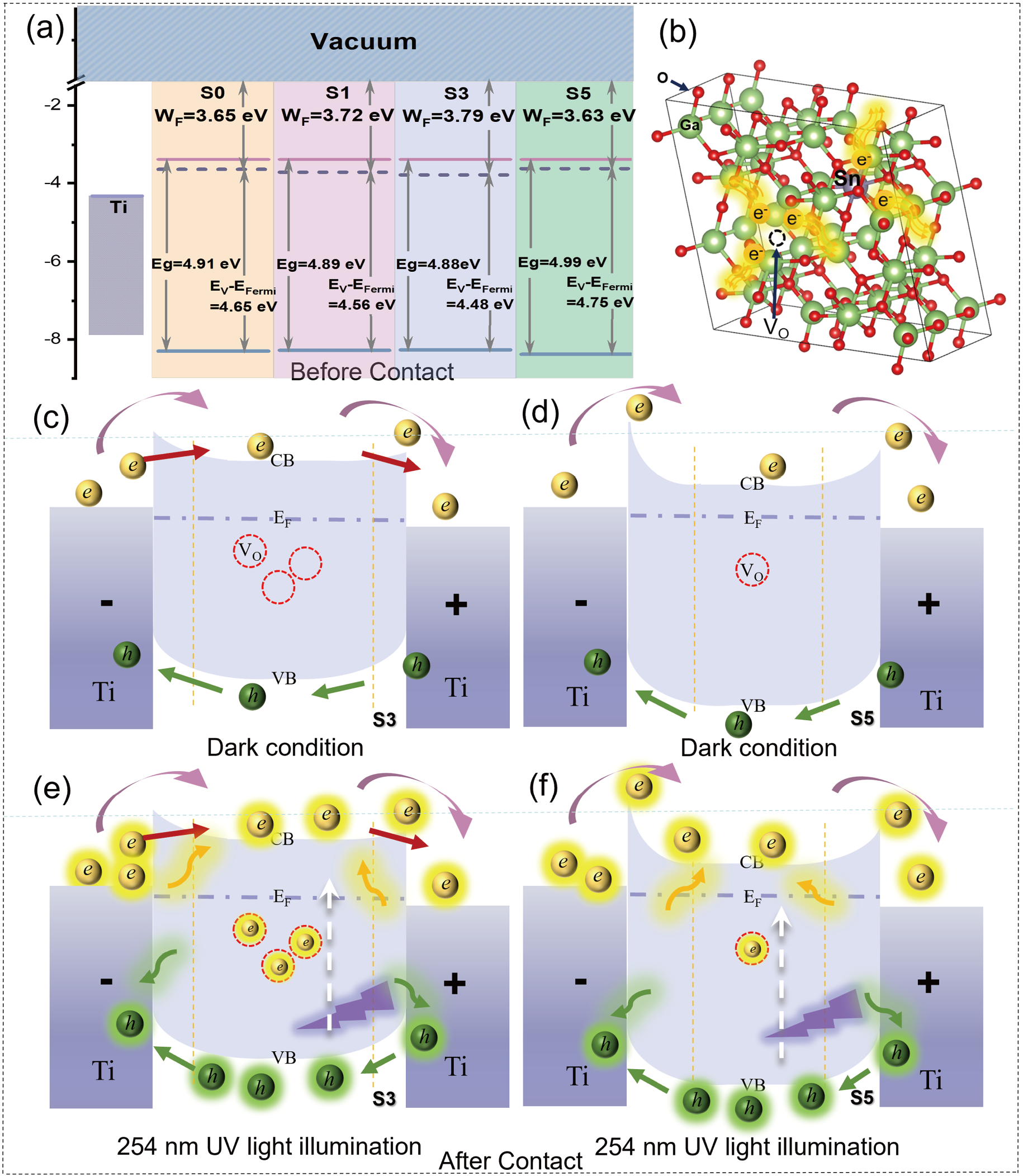
Figure 4. (a) Schematic diagram of energy band structural evolution of S0–S5 samples before contacting with the Ti electrode. (b) Strategy of donor doping to improve conductivity. Operating mechanism of the S3 and S5 devices (c, d) under the dark condition, and (e, f) under UV light illumination with bias after contacting with Ti electrodes.
DOI:
https://doi.org/10.1007/s40843-025-3509-0
