Paper Sharing
【Member Papers】Electronic properties of defects on the (100) casting β-Ga₂O₃: Phenomena and mechanisms
日期:2025-09-22阅读:502
Researchers from the Zhejiang University have published a dissertation titled "Electronic properties of defects on the (100) casting β-Ga2O3: Phenomena and mechanisms" in Applied Surface Science.
Project Support
This work was supported by the National Key Research and Development Program of China (2024YFE0205300), “Pioneer” and “Leading Goose” R&D Program of Zhejiang (2023C01193), the National Natural Science Foundation of China (22205203), the Natural Science Foundation of Zhejiang (LZ25E070001), the National Program for Support of Topnotch Young Professionals, and the Leading Innovative and Entrepreneur Team Introduction Program of Hangzhou (TD2022012).
Background
In this study, three types of defects were revealed on the (100) casting-grown β-Ga2O3 using a 30 wt% KOH etchant. The 3D morphologies and electronic properties of these defects were thoroughly characterized via atomic force microscopy (AFM) and Kelvin probe force microscopy (KPFM). It reveals that voids exhibit the largest local potential gap, followed by dislocation and strain-related defects. Furthermore, emission microscopy images (EMMI) of Schottky barrier diodes (SBDs) prove that reverse leakage current is directly correlated to the type of crystal defects. Voids serve as the major leakage channel under reverse bias, followed by dislocations and strain-related defects, consistent with the KPFM results. Notably, strain-related defects were demonstrated for the first time to degrade the breakdown performance of SBDs, emphasizing the importance of defect control during crystal growth and wafer processing. Finally, the leakage mechanisms on defects were reasonably explained by local potential gaps of different defects combined with a tunneling electronic model within the band-structure. This study deepens the understanding of defect-induced electronic behavior in β-Ga2O3 substrates, clarifies their effects on electrical properties, and provides critical guidance for optimizing crystal growth and improving the performance of power devices.
Abstract
In this study, three types of defects were revealed on the (100) casting-grown β-Ga2O3 using a 30 wt% KOH etchant. The 3D morphologies and electronic properties of these defects were thoroughly characterized via atomic force microscopy (AFM) and Kelvin probe force microscopy (KPFM). It reveals that voids exhibit the largest local potential gap, followed by dislocation and strain-related defects. Furthermore, emission microscopy images (EMMI) of Schottky barrier diodes (SBDs) prove that reverse leakage current is directly correlated to the type of crystal defects. Voids serve as the major leakage channel under reverse bias, followed by dislocations and strain-related defects, consistent with the KPFM results. Notably, strain-related defects were demonstrated for the first time to degrade the breakdown performance of SBDs, emphasizing the importance of defect control during crystal growth and wafer processing. Finally, the leakage mechanisms on defects were reasonably explained by local potential gaps of different defects combined with a tunneling electronic model within the band-structure. This study deepens the understanding of defect-induced electronic behavior in β-Ga2O3 substrates, clarifies their effects on electrical properties, and provides critical guidance for optimizing crystal growth and improving the performance of power devices.
Highlights
● Three types defects on the (100) β-Ga2O3were analyzed using KPFM and validated through EMMI under modulated bias voltages.
● First report of strain-related defects degrades breakdown voltage, underscoring the critical need of defect control.
● Voids were identified the dominant leakage channel, followed by dislocations and strain-related defects.
● The leakage of defects was elucidated with localized potential gaps of defects combined with tunneling electronic model.
Conclusion
In conclusion, we systematically characterized the morphology and electrical properties of three types of etch pits on (100) β-Ga2O3 etched by 30 wt% KOH solution using AFM and KPFM. For the first time, the strain-related defects were shown to exhibit electroactivity, com plementing the previously understood electrical behavior of void- and dislocation-related defects. The results reveal that voids induce the largest local potential gap owing to the presence of donor-like states and significant electron accumulation at the core of void-related etch pits. Additionally, the local potential gap introduced by donor state at the cores of dislocation-related etch pits is approximately twice that of strain-related pits. Furthermore, EMMI technology was used to validate the influence of defects on the breakdown of SBDs, while the sensor validation is outside the scope of this study and will be addressed in future work. All three defect types were found to trigger premature SBD breakdown. Among these, voids significantly lower the breakdown voltage of SBDs, as evidenced by direct visualization of leakage paths under EMMI. In void-free devices, the leakage currents decrease significantly. At this situation, dislocations and strain-related defects sequentially contribute to leakage with the increase of reverse bias, aligning with KPFM results. The influence of the three types of defects on the breakdown of SBDs was reasonably explained via the local potential gaps of defects combined with a tunneling electronic mechanism in band-structure. Dislocations and strain defects act via donor-state- mediated Fermi level shifts, amplifying band bending and enhancing tunneling probability. In comparative, both the positive and negative potential gap at the core of voids contribute to a tunneling effect com bined with an electric field strength concentration, that is, electron accumulation leakage mechanism, explaining the easy breakdown of SBDs at the position of voids. These results establish the defect impact order of voids-, dislocations- and strain-related defects and highlight the need to control all three types of defects during crystal growth and subsequent wafer processing. This work advances understanding of defect-driven electron transport in (100) β-Ga2O3, directly supporting its application in ultra-high power devices.
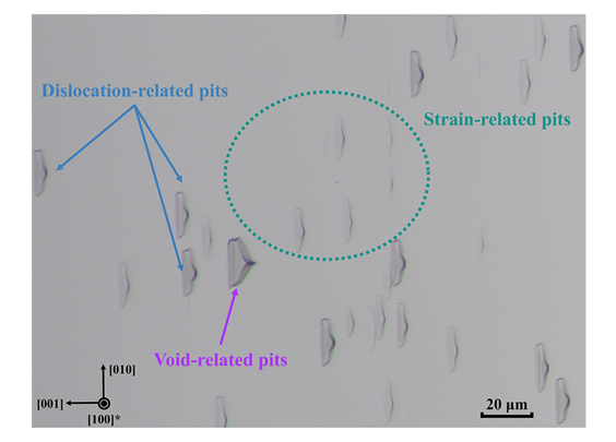
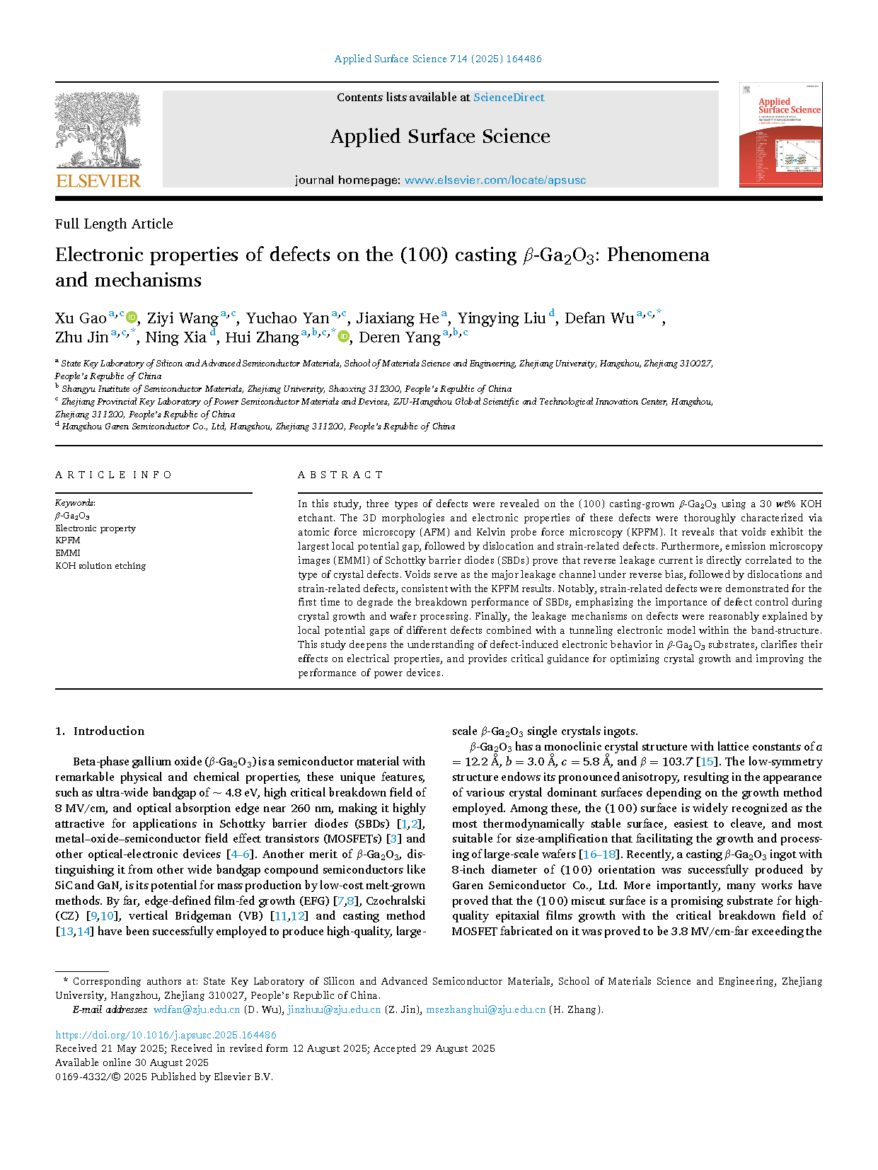
Fig. 1. OM images for three types etch pits on the (100) β-Ga2O3 substrate etched by 30 wt% KOH solution for 1.5 h at 110 ℃.
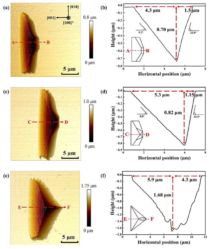
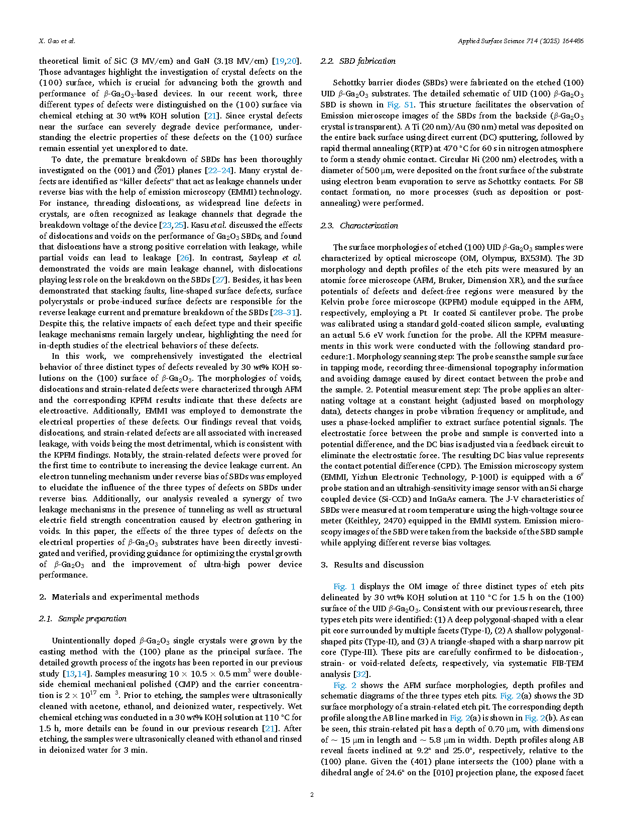
Fig. 2. Surface morphologies, depth profiles of representative (a-b) strain-related etch pit, (c-d) dislocation-related etch pit and (e-f) void-related etch pit and inserts are the schematic diagrams.
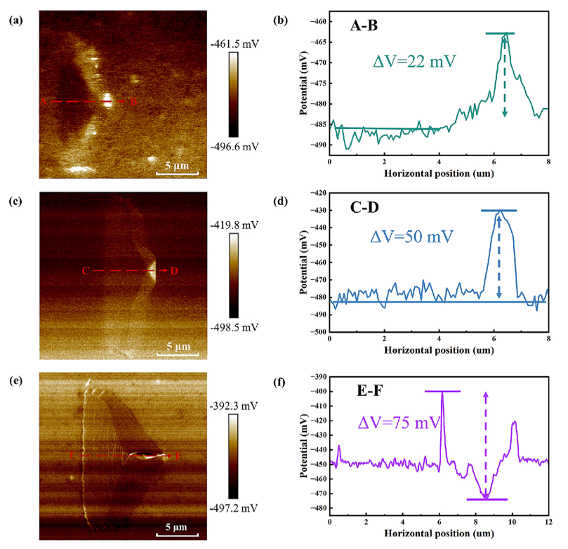
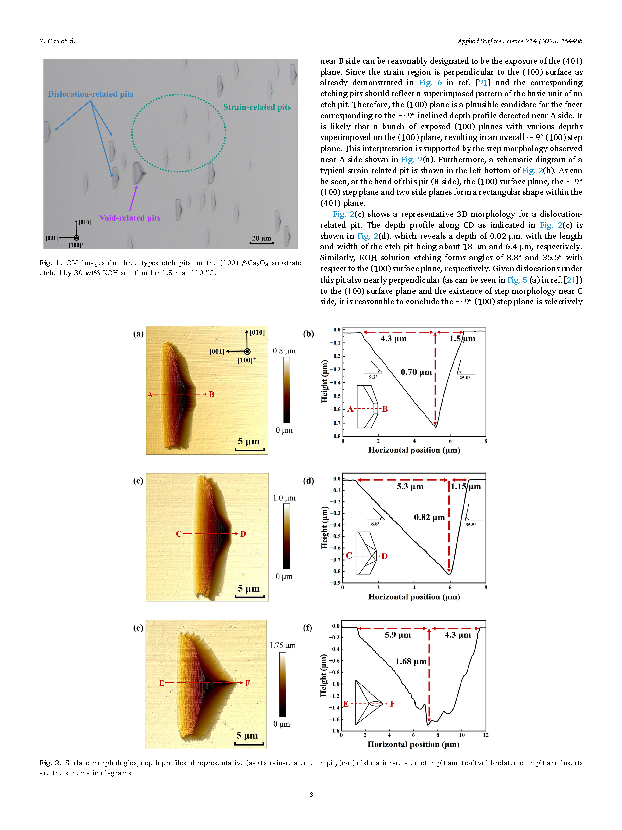
Fig. 3. Surface potential mapping images of containing the etch pit and the line profiles for the surface potentials across the etch pit of (a-b) for strain-related etch pit, (c-d) for dislocation-related etch pit, and (e-f) for void-related etch pit.
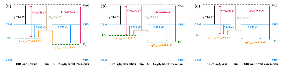
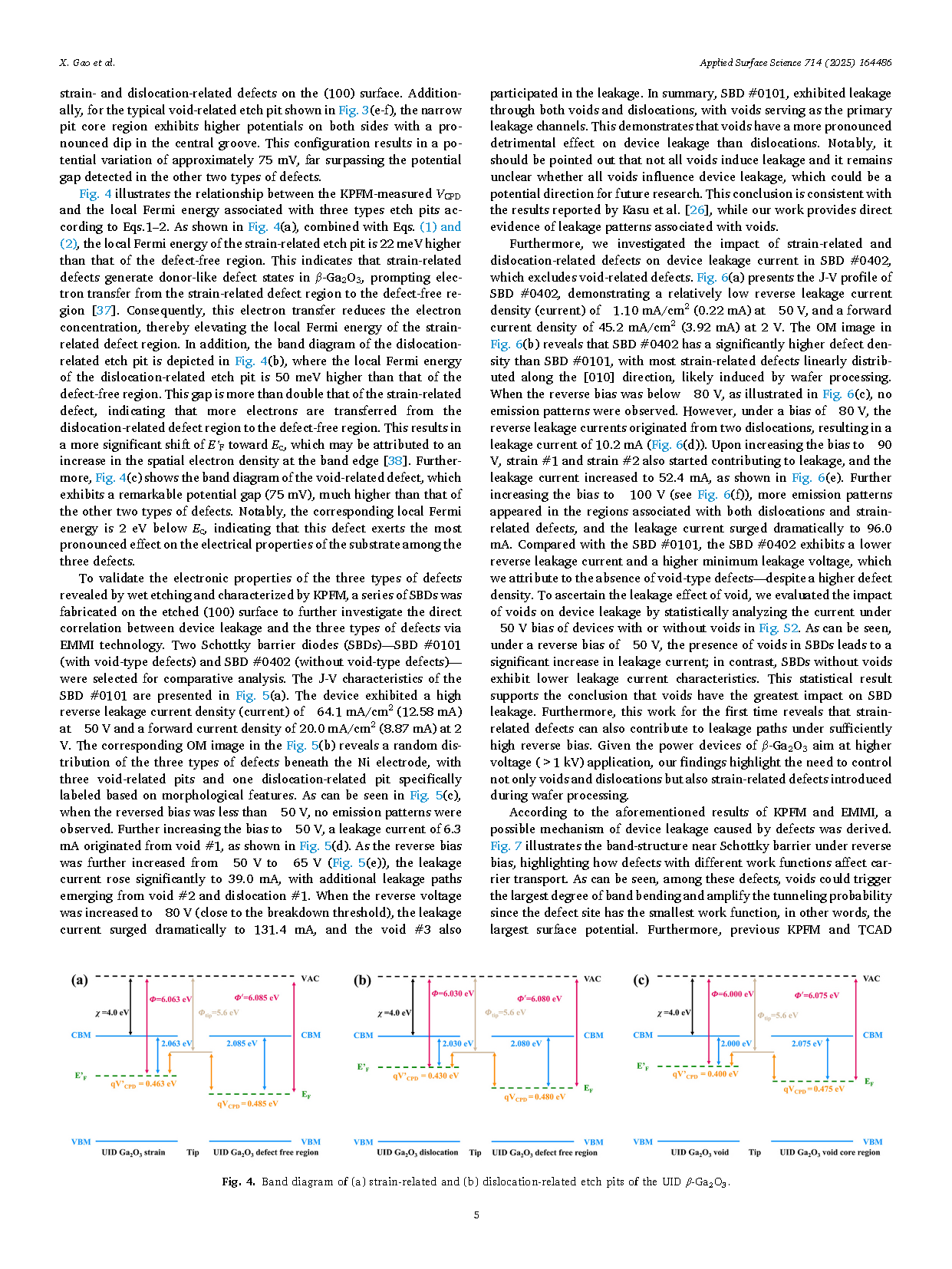
Fig. 4. Band diagram of (a) strain-related and (b) dislocation-related etch pits of the UID β-Ga2O3.
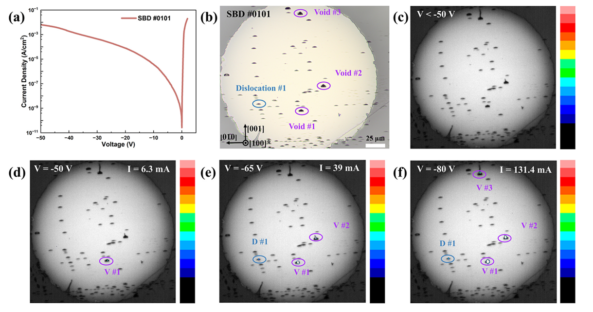
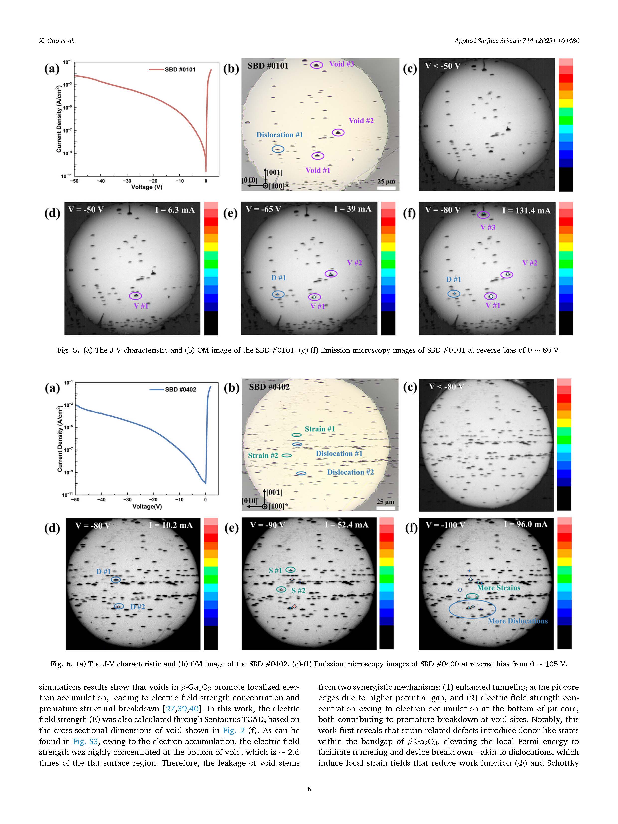
Fig. 5. (a) The J-V characteristic and (b) OM image of the SBD #0101. (c)-(f) Emission microscopy images of SBD #0101 at reverse bias of 0 ~ 80 V.
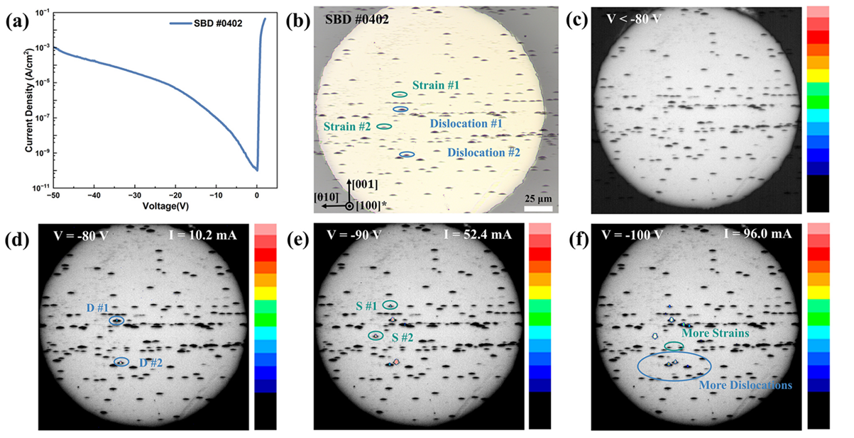
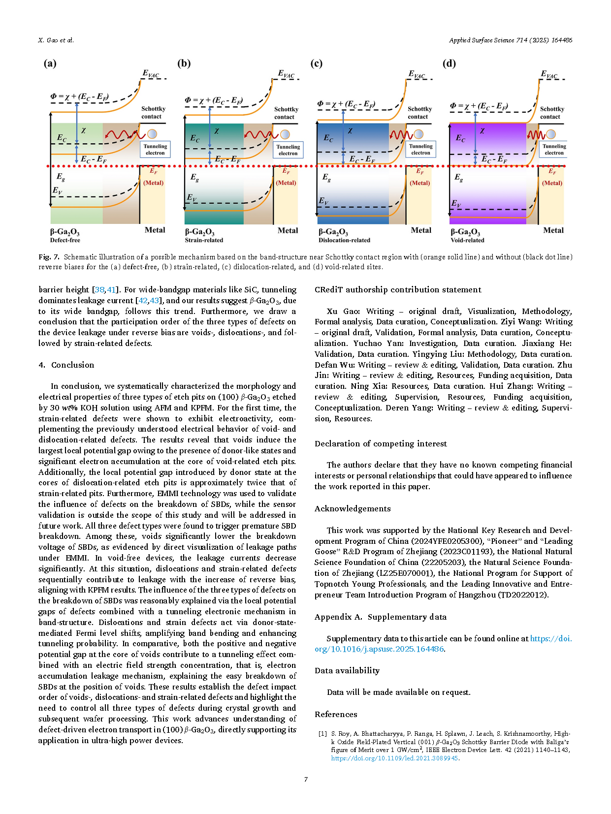
Fig. 6. (a) The J-V characteristic and (b) OM image of the SBD #0402. (c)-(f) Emission microscopy images of SBD #0400 at reverse bias from 0 ~ 105 V.
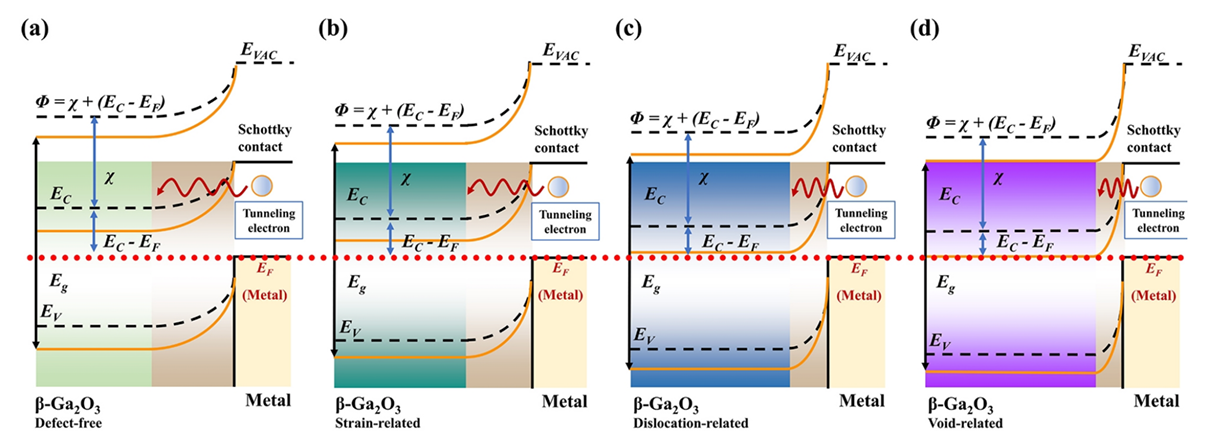
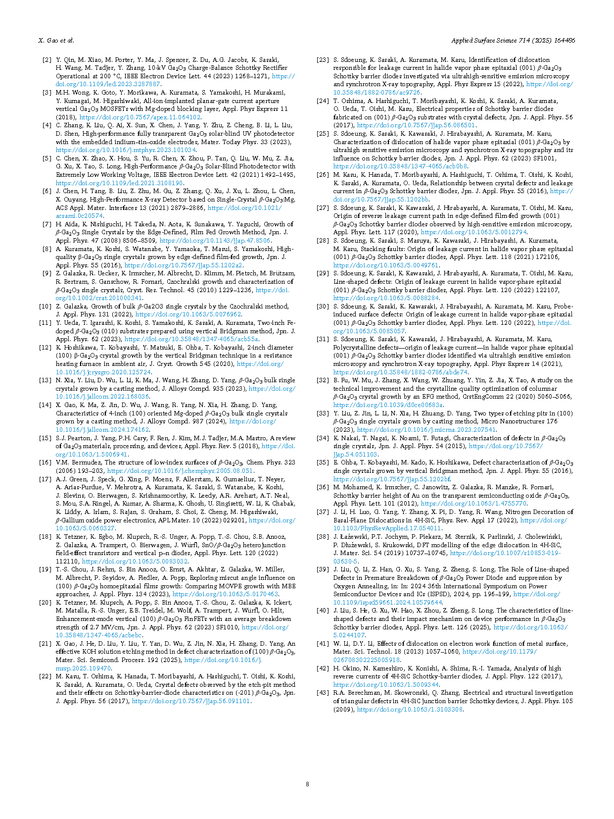
Fig. 7. Schematic illustration of a possible mechanism based on the band-structure near Schottky contact region with (orange solid line) and without (black dot line) reverse biases for the (a) defect-free, (b) strain-related, (c) dislocation-related, and (d) void-related sites.
DOI:
doi.org/10.1016/j.apsusc.2025.164486