Paper Sharing
【International Papers】Planar Defects and Structural Heterogeneity in Ultrawide Bandgap Semiconductors
日期:2025-08-22阅读:547
Researchers from the Arizona State University have published a dissertation titled "Planar Defects and Structural Heterogeneity in Ultrawide Bandgap Semiconductors" in Microscopy and Microanalysis.
Abstract
Ultrawide bandgap (UWBG) semiconductors, such as diamond, BN and β-Ga2O3, exhibit exceptional properties that make them highly attractive for high-voltage and high-frequency power electronics. Despite their superior physical and, in many cases, exceptional thermal properties, device fabrication is challenging. Hetero-integration of UWBG materials represents a promising approach to overcoming some difficulties. For example, p-type doping of β-Ga2O3 and n-type doping of diamond are hard to accomplish, whereas integration can leverage the easily achieved doping configurations of each separate material. Moreover, the extremely high thermal conductivity of diamond helps address thermal management challenges associated with poor heat conducting materials. Recent studies of polycrystalline (PC) diamond, which has reasonably high thermal conductivity compared to other widely used semiconductors, shows promising results as a heat-spreading layer for device integration. In this work, we have characterized microstructural features observed in UWBG semiconductor layers, focusing on planar defects and select 3D features mostly comprising planar defects. The samples studied include PC-diamond layers grown on Si substrates for thermal management applications, and β-Ga2O3 layers grown on diamond substrates for high-power electronics. High-resolution transmission electron microscopy (HRTEM) and convergent beam electron diffraction (CBED)/nano-beam diffraction were used to assess structural homogeneity, lattice distortion, and strain distribution across the planar defects.
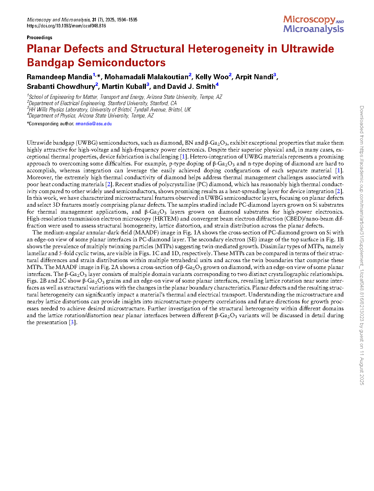
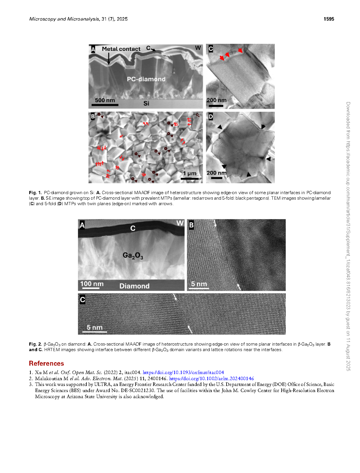
The medium-angular annular-dark-field (MAADF) image in Fig. 1A shows the cross-section of PC-diamond grown on Si with an edge-on view of some planar interfaces in PC-diamond layer. The secondary electron (SE) image of the top surface in Fig. 1B shows the prevalence of multiply twinning particles (MTPs) suggesting twin-mediated growth. Dissimilar types of MTPs, namely lamellar and 5-fold cyclic twins, are visible in Figs. 1C and 1D, respectively. These MTPs can be compared in terms of their structural differences and strain distributions within multiple tetrahedral units and across the twin boundaries that comprise these MTPs. The MAADF image in Fig. 2A shows a cross-section of β-Ga2O3 grown on diamond, with an edge-on view of some planar interfaces. The β-Ga2O3 layer consists of multiple domain variants corresponding to two distinct crystallographic relationships. Figs. 2B and 2C show β-Ga2O3 grains and an edge-on view of some planar interfaces, revealing lattice rotation near some interfaces as well as structural variations with the changes in the planar boundary characteristics. Planar defects and the resulting structural heterogeneity can significantly impact a material’s thermal and electrical transport. Understanding the microstructure and nearby lattice distortions can provide insights into microstructure-property correlations and future directions for growth processes needed to achieve desired microstructure. Further investigation of the structural heterogeneity within different domains and the lattice rotation/distortion near planar interfaces between different β-Ga2O3 variants will be discussed in detail during the presentation.
Fig. 1. PC-diamond grown on Si: A. Cross-sectional MAADF image of heterostructure showing edge-on view of some planar interfaces in PC-diamond layer. B. SE image showing top of PC-diamond layer with prevalent MTPs (lamellar: red arrows and 5-fold: black pentagons). TEM images showing lamellar (C) and 5-fold (D) MTPs with twin planes (edge-on) marked with arrows.

Fig. 2. β-Ga2O3 on diamond: A. Cross-sectional MAADF image of heterostructure showing edge-on view of some planar interfaces in β-Ga2O3 layer. B and C. HRTEM images showing interface between different β-Ga2O3 domain variants and lattice rotations near the interfaces.
DOI:
doi.org/10.1093/mam/ozaf048.816