Paper Sharing
【International Papers】Enhanced UVC Responsivity of Heteroepitaxial α-Ga₂O₃ Photodetector with Ultra-Thin HfO₂ Interlayer
日期:2025-08-13阅读:534
Researchers from the Soongsil University have published a dissertation titled " Enhanced UVC Responsivity of Heteroepitaxial α-Ga2O3 Photodetector with Ultra-Thin HfO2 Interlayer " in Micromachines.
Background
Ultraviolet (UV) detection is crucial for a wide range of applications, including fire detection, sterilization, environmental monitoring, aerospace, and defense systems. Within the UV spectrum, high-energy UVC radiation (wavelength < 280 nm) is particularly significant in extreme environments. However, its carcinogenic nature and capacity to cause severe DNA damage pose significant risks to biological systems, including human skin and eyes. Although the stratospheric ozone layer effectively absorbs most UVC radiation, the selective detection of weak UVC signals under visible or solar illumination remains a considerable technical challenge. Therefore, the development of highly sensitive and selective UVC detectors capable of operating in solar environments is essential for advancing these critical applications.
Conventional wide-bandgap semiconductors, such as aluminum gallium nitride (AlGaN) and diamond, have long been considered for UVC detection. Yet, AlGaN faces challenges in achieving high-quality thin films because of the complexities of its ternary alloy system, whereas diamond, despite its exceptional intrinsic properties, is hindered by its high fabrication cost and limited scalability for large-area integration.
Abstract
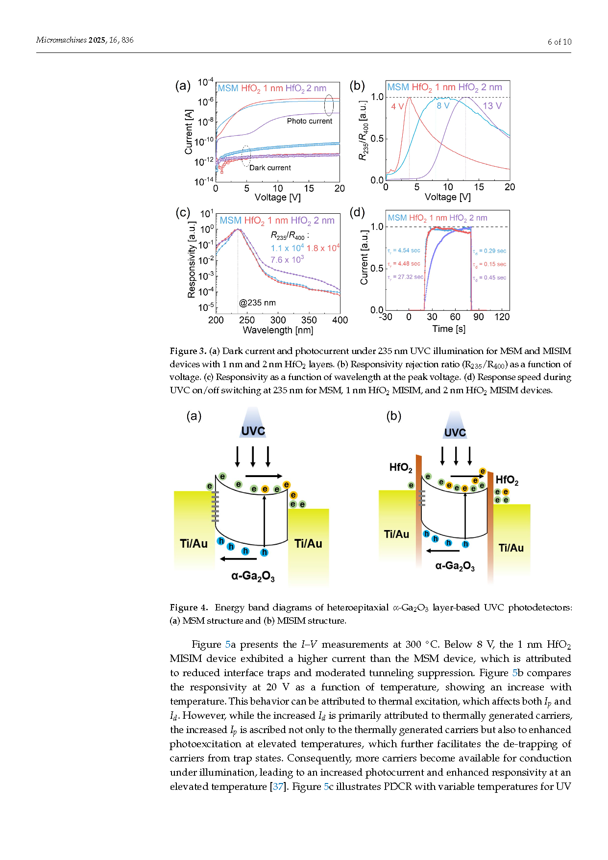
In this study, the influence of HfO2 interlayer thickness on the performance of heteroepitaxial α-Ga2O3 layer-based metal–insulator–semiconductor–insulator–metal (MISIM) ultraviolet photodetectors is examined. A thin HfO2 interlayer enhances the interface quality and reduces the density of interface traps, thereby improving the performance of UVC photodetectors. The fabricated device with a 1 nm HfO2 interlayer exhibited a significantly reduced dark current and higher photocurrent than a conventional metal–semiconductor–metal (MSM). Specifically, the 1 nm HfO2 MISIM device demonstrated a photocurrent of 2.3 μA and a dark current of 6.61 pA at 20 V, whereas the MSM device exhibited a photocurrent of 1.1 μA and a dark current of 73.3 pA. Furthermore, the photodetector performance was comprehensively evaluated in terms of responsivity, response speed, and high-temperature operation. These results suggest that the proposed ultra-thin HfO2 interlayer is an effective strategy for enhancing the performance of α-Ga2O3-based UVC photodetectors by simultaneously suppressing dark currents and increasing photocurrents and ultimately demonstrate its potential for stable operation under extreme environmental conditions.
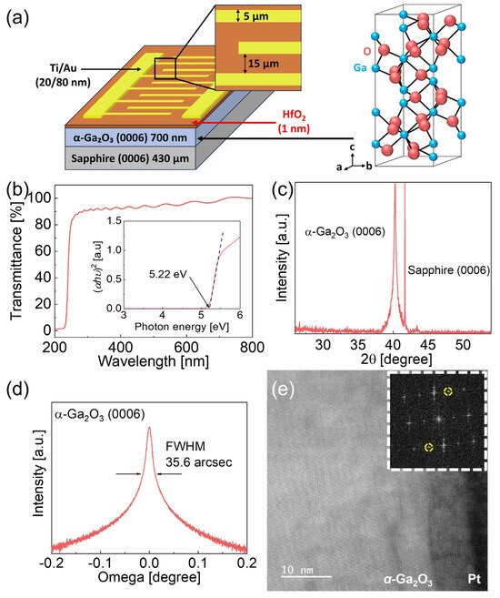
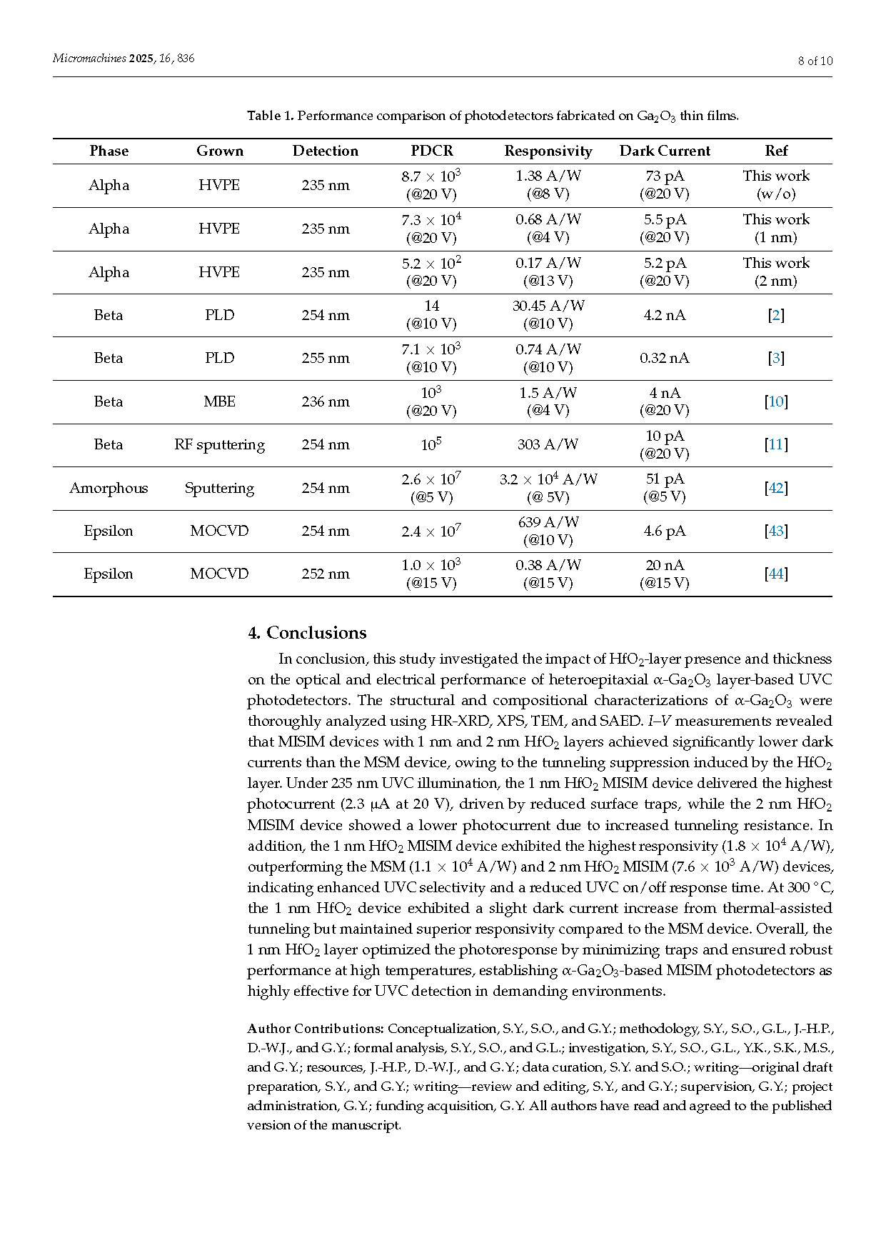
Figure 1. (a) Schematic of the MISIM photodetector, featuring an HfO2 insulating layer on α-Ga2O3 and a 3D schematic diagram of the α-Ga2O3 lattice structure. (b) Optical transmittance spectrum with an inset showing the optical bandgap of the heteroepitaxial α-Ga2O3 layer, estimated using a Tauc plot. (c) High-resolution X-ray diffraction (HR-XRD) 2θ scan of the heteroepitaxial α-Ga2O3 layer. (d) HR-XRD rocking curve for the (0006) diffraction peak. (e) Cross-view transmission electron microscope (TEM) image of α-Ga2O3 thin film with an inset selected area electron diffraction pattern.
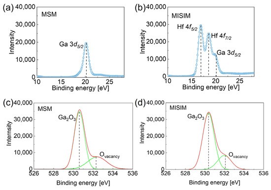
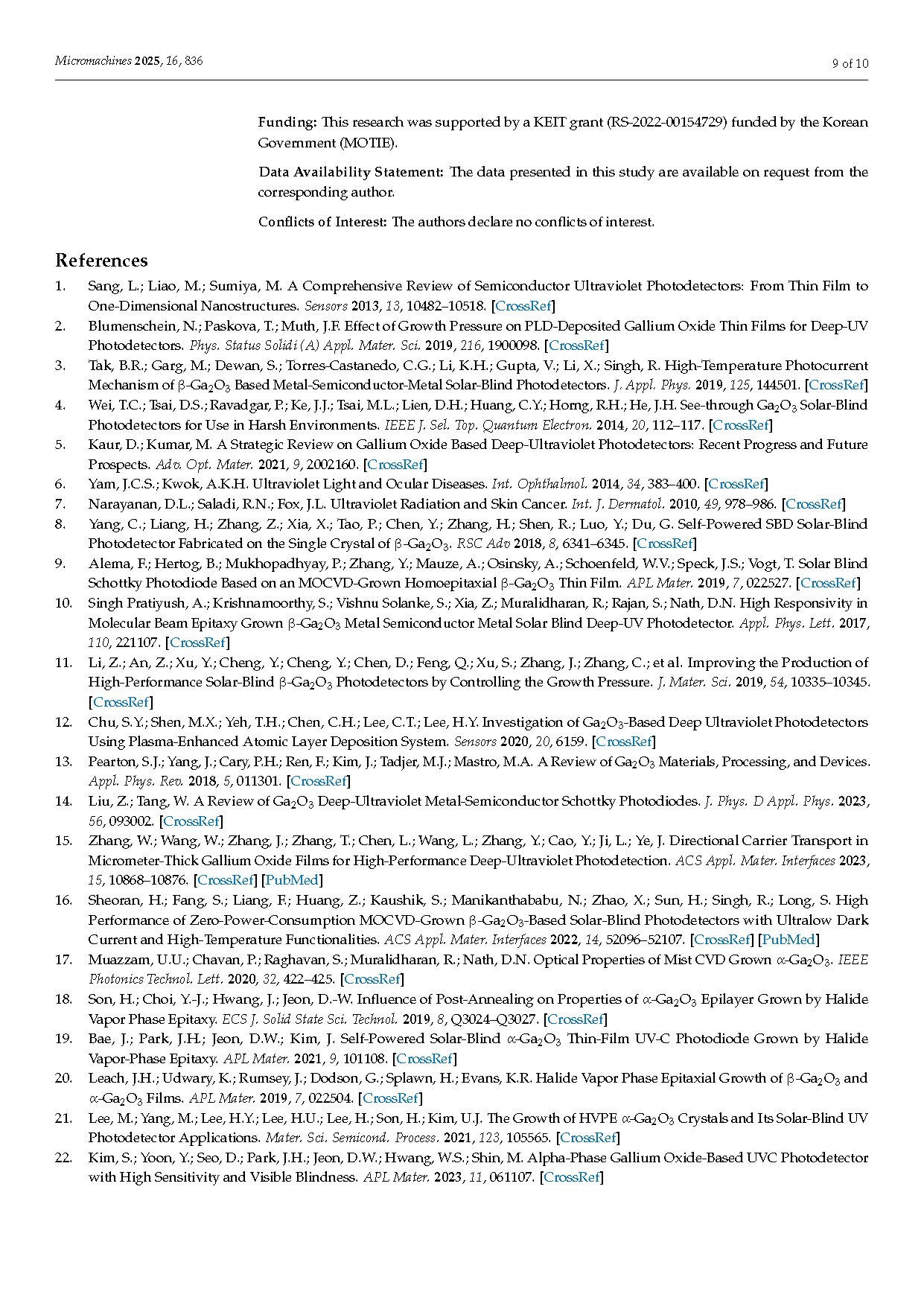
Figure 2. (a) XPS spectrum of Ga 3d5/2 for the MSM structure; (b) XPS spectra of Hf 4f5/2, Hf 4f7/2, and Ga 3d5/2 for the MISIM structure. The O 1s XPS spectrum (c) for the MSM structure and (d) for the MISIM structure, showing Ga2O3 and oxygen vacancies.
DOI:
doi.org/10.3390/mi16070836