Paper Sharing
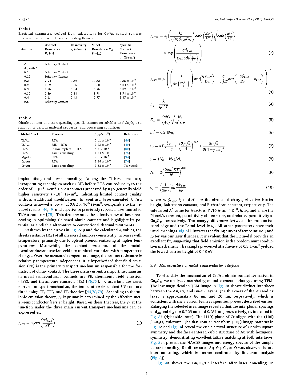
【Member Papers】Unveiling the interfacial nanostructure and electrical mechanism of low-resistivity Cr/Au ohmic contacts formed on β-Ga₂O₃ via laser annealing
日期:2025-08-12阅读:524
Researchers from the Fudan University have published a dissertation titled "Unveiling the interfacial nanostructure and electrical mechanism of low-resistivity Cr/Au ohmic contacts formed on β-Ga2O3 via laser annealing" in Applied Surface Science.
Project Support
This work is supported by the National Key R&D Program of China (2023YFB4606300), the Joint Research Plan of sci-tech innovation community in Yangtze River Delta (No.2023CSJG0600), the Science and Technology Innovation Plan of Shanghai Science and Technology Commission (No. 21DZ1100800, 23ZR1405300, 20501110700, and 20501110702), the National Natural Science Foundation of China (52302202), the Science and Technology Major Project of Ningbo (2021Z123), the Yongjiang Talent Introduction Programme of Ningbo (2021A-037-C, 2021A-108-G), and the Youth Fund of the Chinese Academy of Sciences (No. JCPYJJ22030).
Background
Gallium oxide (Ga2O3) has been proposed as the ultra-wide bandgap semiconductor material for next-generation power electronics and optoelectronic devices due to its wider band gap, higher breakdown field, and higher Baliga’s Figure of Merit (BFOM) than GaN and SiC. The breakdown voltage of Ga2O3 Schottky barrier diodes (SBDs) and Metal-Oxide-Semiconductor Field Effect Transistors (MOSFETs) has exceeded the theoretical limit of GaN and SiC. The ohmic contact, which forms the critical interface between the semiconductor and the metal electrode, plays a key role in determining the performance of the electrical device. For high-performance power devices requiring minimal voltage loss and reduced energy dissipation, it is essential to fabricate an ideal ohmic contact with low specific contact resistance and good thermal stability between metal and semiconductor, since these two properties are often challenging to achieve simultaneously. Although RTA is crucial for the formation of Ga2O3 ohmic contacts, its process sequence negatively affects Schottky contacts during device fabrication. Considering the heat budget and heat-affected region, RTA can lead to a reduction in the reverse breakdown voltage of SBD, a decrease in channel mobility, and an increase in the threshold voltage of MOSFETs. The annealing equipment used in the RTA process operates in a non-enclosed environment and lacks spatial selectivity in the annealing region, resulting in epitaxial layer stress and high-temperature thermal damage. Moreover, the lack of uniformity and stability in the RTA process can easily cause thermal damage in other areas of the device, resulting in lattice defects or lateral diffusion of dopant atoms. Consequently, laser annealing technology, which is based on laser heat treatment, has gradually emerged as a research focus. In the semiconductor industry, lasers are commonly used for dicing, thinning, marking, and several other processes. A pulsed laser is widely used for the annealing process in the Si, GaAs, SiC, and GaN devices. The process of establishing ohmic contact involves pulsed laser annealing, which selectively heats only the laser-irradiated region on the contact surface. This localized heating induces a reaction between the substrate and the contact metal, enabling ohmic contact while preserving the overall electrical properties of the substrate due to the short annealing time and limited irradiation area. In the case of Ga2O3, the impact of laser annealing on metal/Ga2O3 interface properties, particularly in the context of ohmic contact formation, remains insufficiently studied.
Abstract
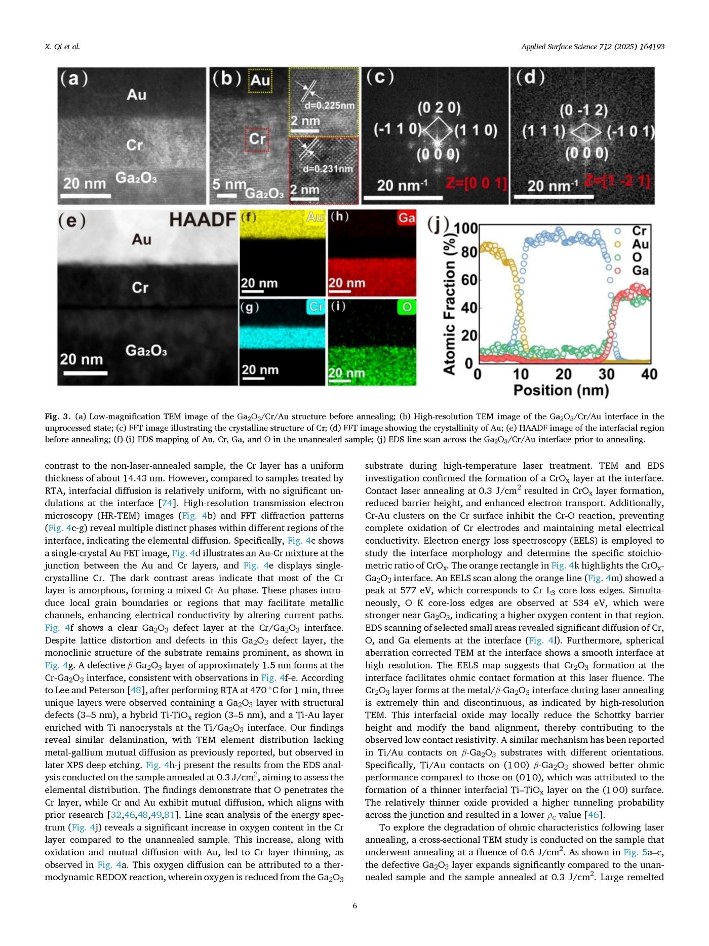
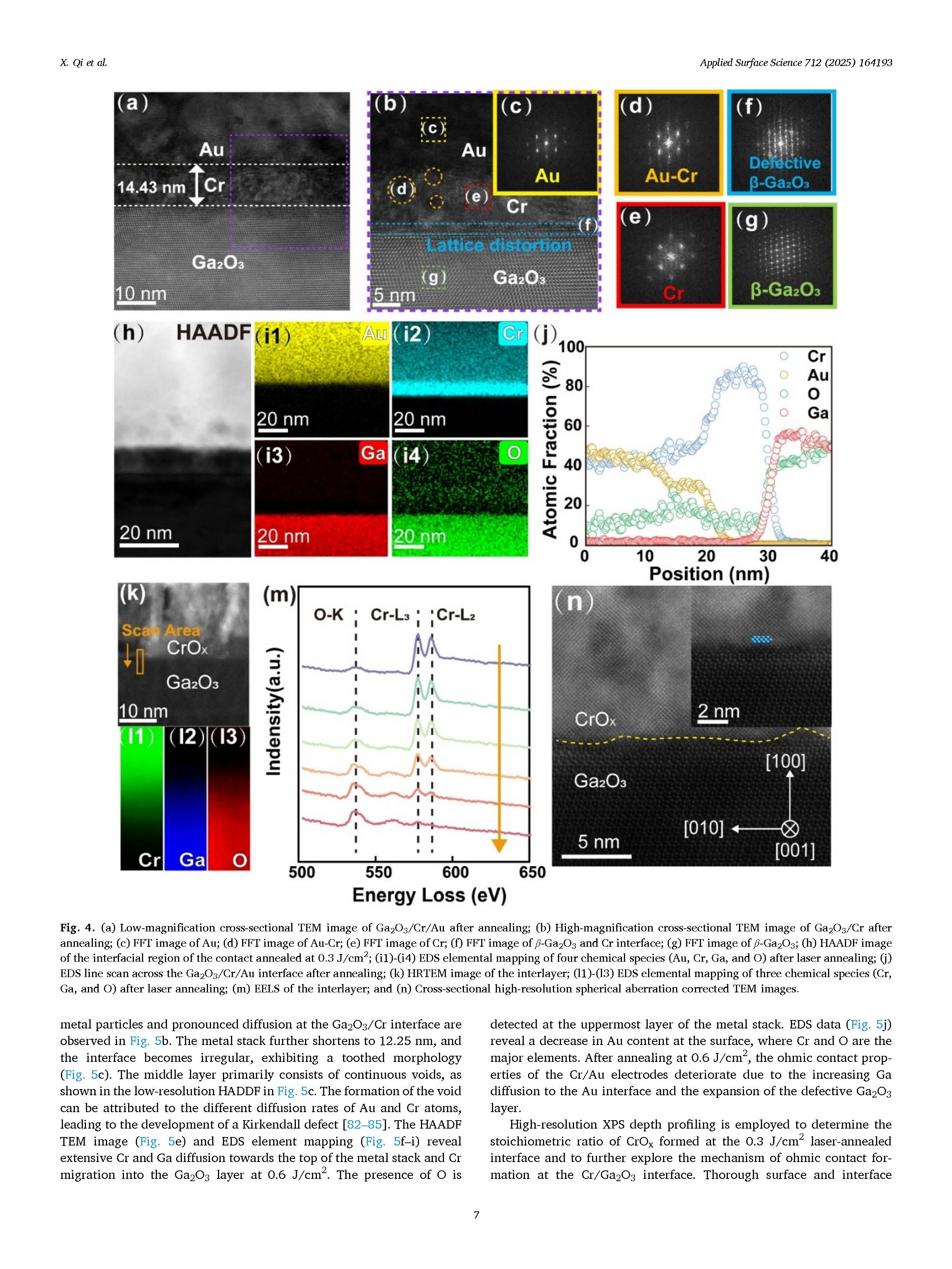
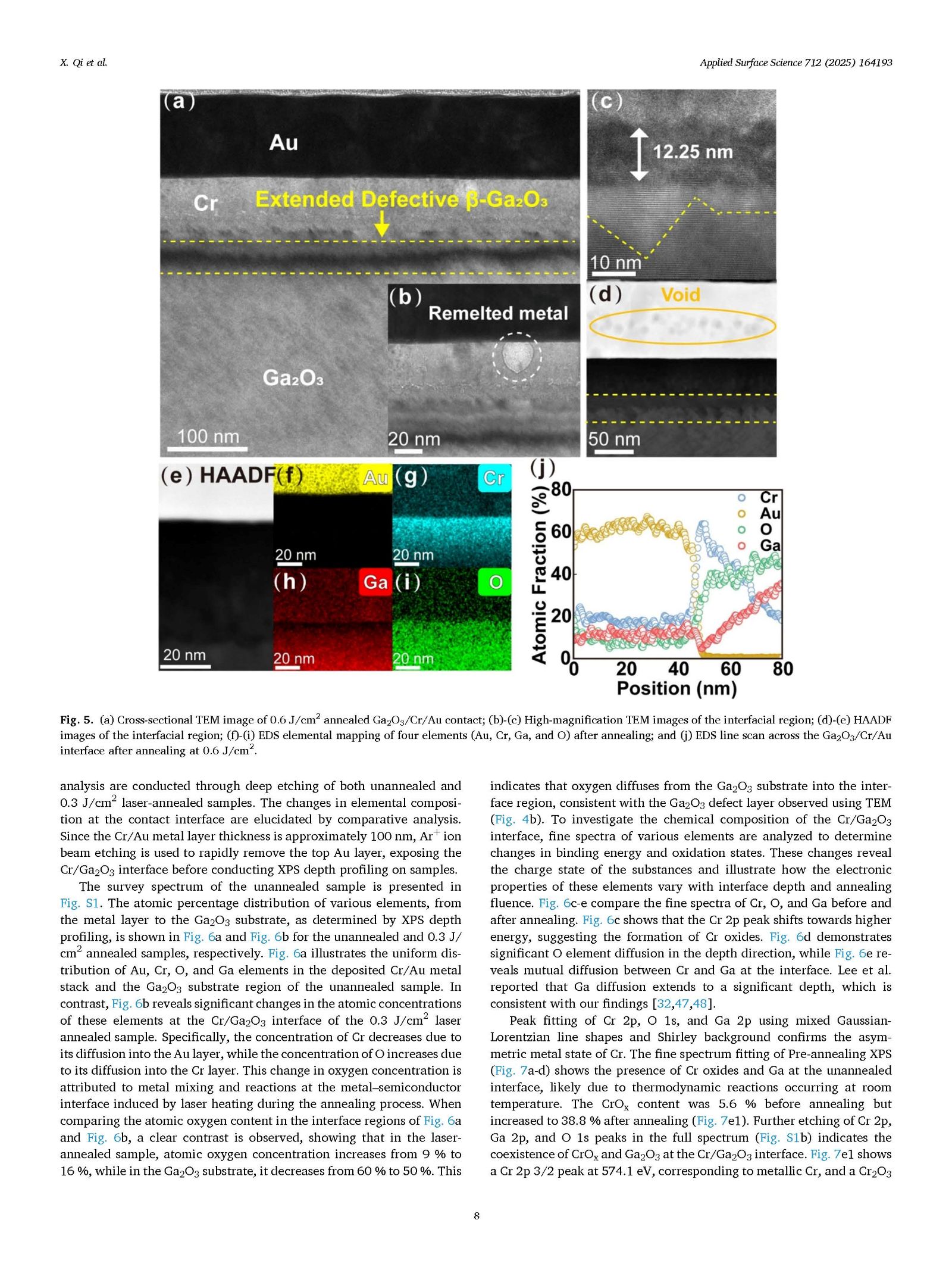
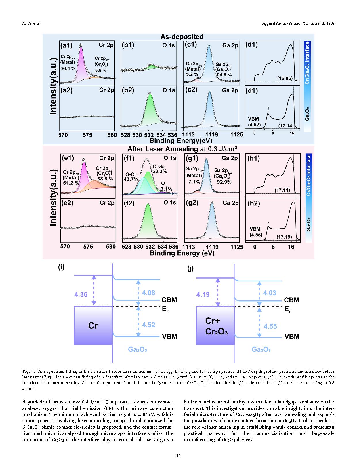
The ultra-wide band-gap semiconductor gallium oxide (Ga2O3) holds great potential for the development of high-voltage, high-power, and low-loss power devices, as well as optoelectronic applications. However, the performance of Ga2O3-based devices falls significantly short of expectations, largely due to the substantial Schottky barrier height and contact resistance at the metal-Ga2O3 interface. This study adapts and optimizes laser annealing for β-Ga2O3, replacing conventional RTA to achieve ohmic contact formation. The influence of varying annealing fluence on the electrical properties and interfacial reactions is analyzed. After annealing at fluences ranging from 0.1 to 0.6 J/cm2 at 1 kHz, the lowest specific contact resistance(ρc) of 3.82 × 10⁻⁵ Ω·cm2 is achieved at 0.3 J/cm2. Temperature-dependent contact analyses indicate that field emission (FE) is the dominant conduction mechanism. The lowest extracted barrier height is 0.48 eV. After conducting electrical testing, material characterization, and theoretical analysis, it is evident that the development of an ohmic contact is primarily driven by the formation of a Cr2O3 layer with a reduced bandgap at the metal-Ga2O3 interface. The interface is flatter and has a smaller affected area than the ohmic contacts formed by RTA, and the process results in more efficient interdiffusion and chemical reactions between the metal and the semiconductor, making Ga2O3 power devices more commercially viable.
Highlights
● Laser annealing is explored as a promising technique for Ga2O3 ohmic contact formation.
● The low specific contact resistivity 3.82 × 10⁻⁵ Ω ∙ cm2 has achieved which falls within the range of ideal ohmic contact.
● The interfacial diffusion of Cr and Ga, along with O diffusion, facilitates the establishment of ohmic contact.
● Interfacial discontinuous Cr2O3 formed during laser annealing reduces the Schottky barrier, facilitating ohmic contact formation on β-Ga2O3.
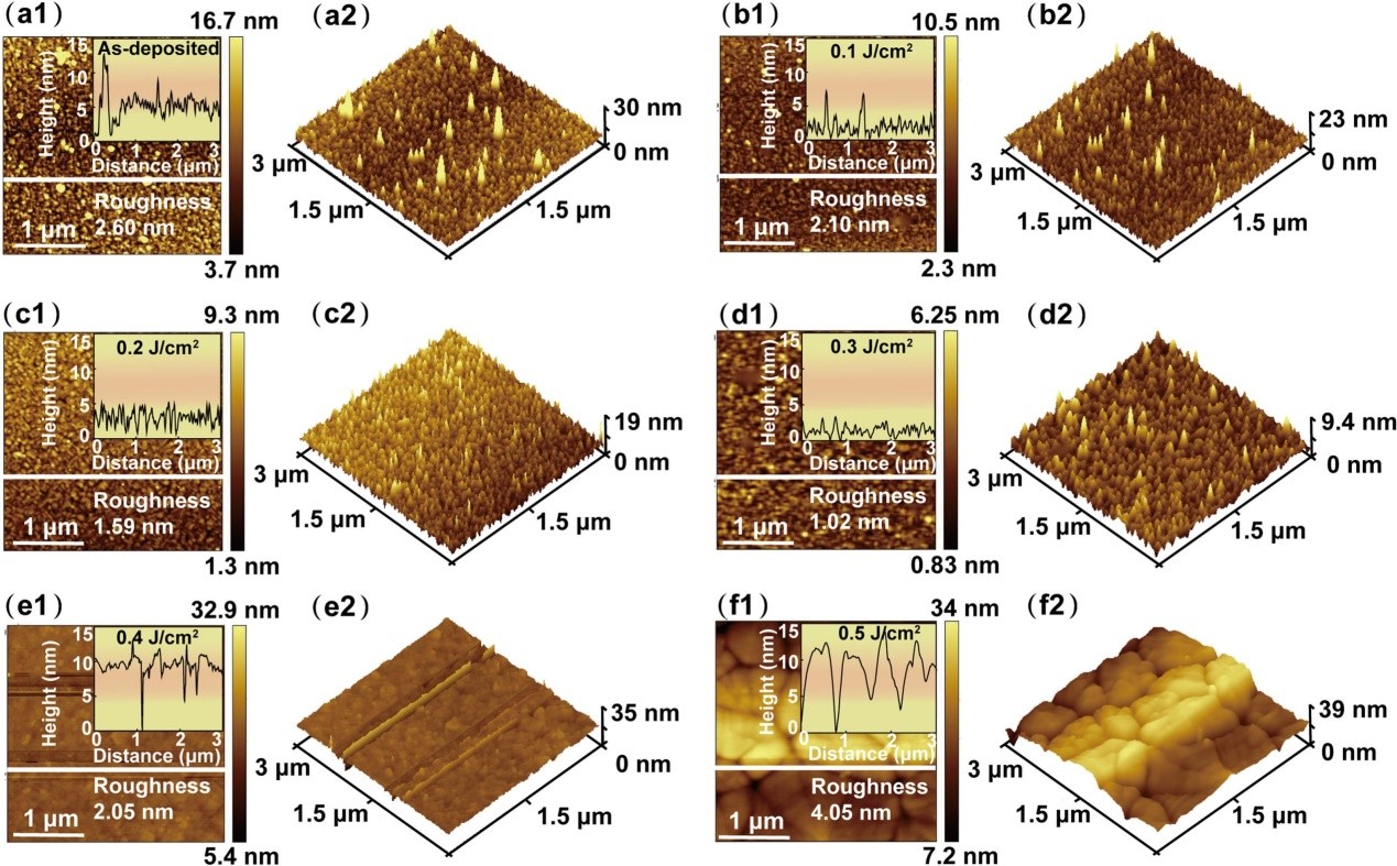
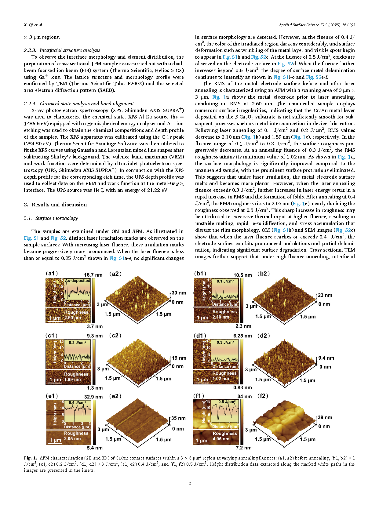
Fig. 1. AFM characterization (2D and 3D) of Cr/Au contact surfaces within a 3×3 μm2 region at varying annealing energy densities: (a1, a2) before annealing, (b1, b2) 0.1 J/cm2, (c1, c2) 0.2 J/cm2, (d1, d2) 0.3 J/cm2, (e1, e2) 0.4 J/cm2, and (f1, f2) 0.5 J/cm2. Height distribution data extracted along the marked white paths in the images are presented in the insets.

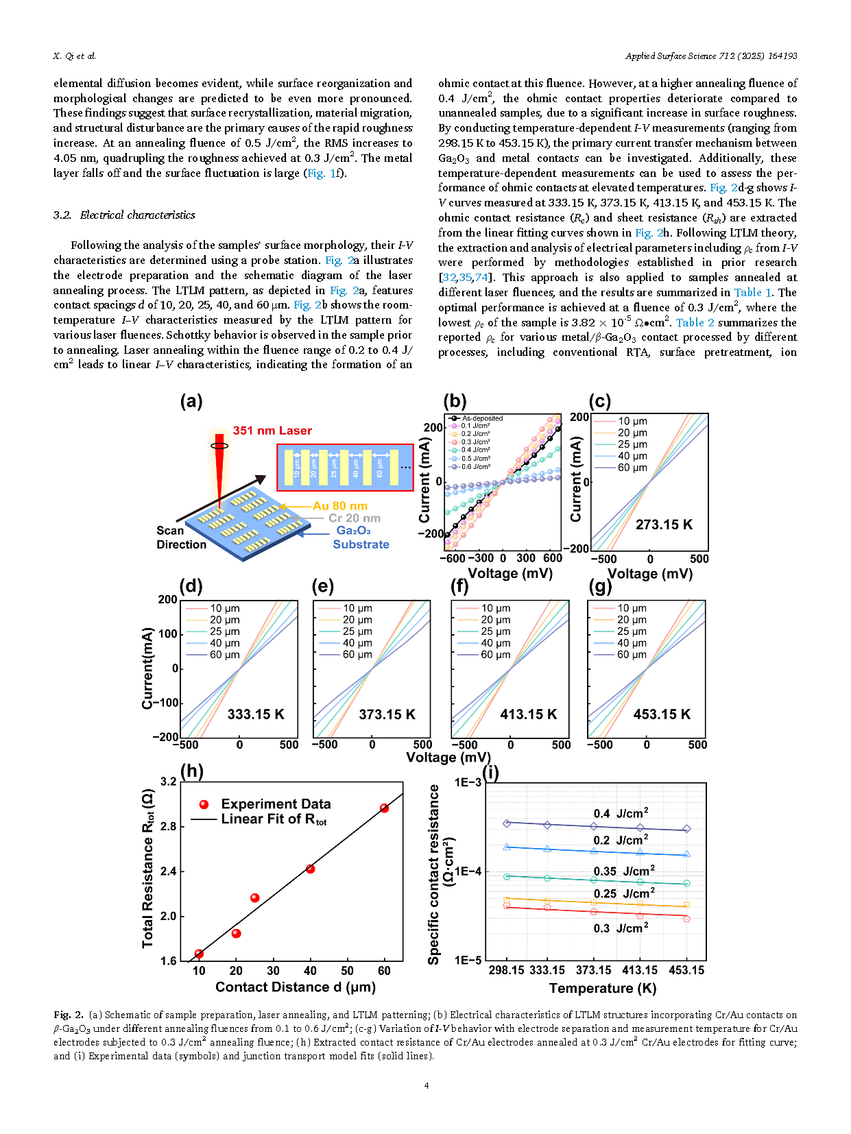
Fig. 2. (a) Schematic of sample preparation, laser annealing, and LTLM patterning; (b) Electrical characteristics of LTLM structures incorporating Cr/Au contacts on β-Ga2O3 under different annealing fluences from 0.1 to 0.6 J/cm2 ; (c-g) Variation of I-V behavior with electrode separation and measurement temperature for Cr/Au electrodes subjected to 0.3 J/cm2 annealing fluence; (h) Extracted contact resistance of Cr/Au electrodes annealed at 0.3 J/cm2 Cr/Au electrodes for fitting curve; and (i) Experimental data (symbols) and junction transport model fits (solid lines).
DOI:
doi.org/10.1016/j.apsusc.2025.164193