Paper Sharing
【International Papers】Substrate-orientation dependence of β-Ga₂O₃ nitridation by RF nitrogen plasma for GaN heterojunction diodes
日期:2025-08-12阅读:475
Researchers from the University of Illinois Urbana-Champaign have published a dissertation titled "Substrate-orientation dependence of β-Ga2O3 nitridation by RF nitrogen plasma for GaN heterojunction diodes" in Journal of Applied Physics.
Background
β-Gallium oxide (Ga2O3) has been implemented for power and optical microelectronic devices, demonstrating high purity and high crystallinity with controllable n-type doping. However, p-type doping has not been demonstrated to the degree of control required for power devices. Given the extremely low dispersion leading to large hole effective mass, generated holes are polaronic in nature and are unable to contribute meaningfully to conduction. As an alternative, heterojunction devices have been explored, with demonstrated success in p-type gallium nitride (p-GaN). GaN-β-Ga2O3 heterojunctions have complementary properties, both are classified as wide (or ultra-wide) bandgap, and have high electron saturation velocity and large critical field strength. Furthermore, GaN has a robust p-type dopant in the form of magnesium (Mg).
Abstract
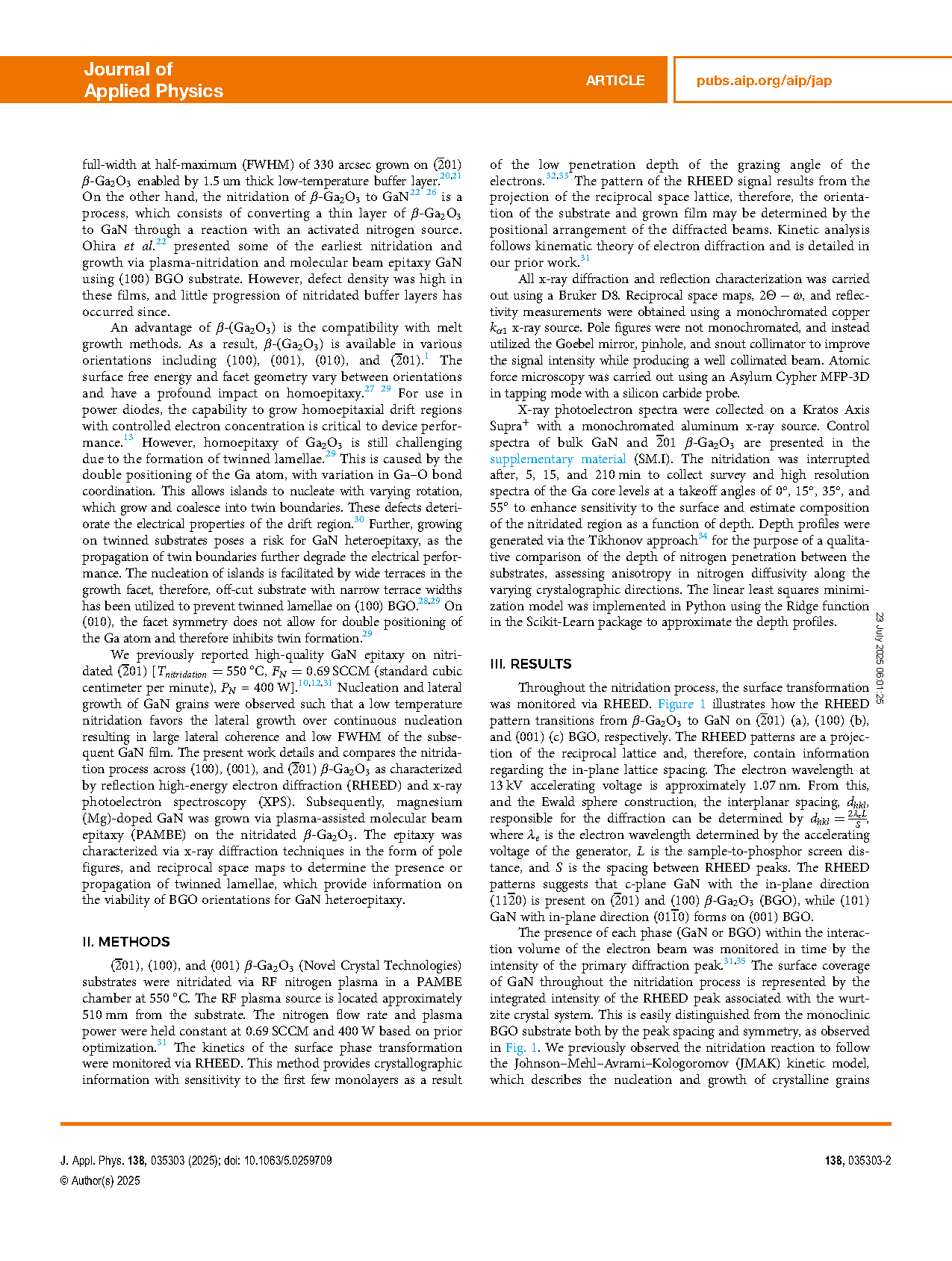
The influence of substrate orientation on the structural properties of heteroepitaxial GaN films grown on nitridated β-Ga2O3 (BGO) is investigated. The nitridation of (100), (001), and (-201) β-Ga2O3 was monitored with reflection high energy electron diffraction and x-ray photoelectron spectroscopy, suggesting the reaction proceeds through the formation of an oxynitride phase in all cases. The nitridation rate (Γ) under fixed nitridation conditions was observed to increase monotonically with the inverse of the surface free energy of the starting substrate, Γ(001) < Γ(-201) < Γ(100). Hexagonal GaN is realized on all orientations, however, (001) BGO nucleates an undesired (101) plane GaN interface. The presence of restructured BGO grains is also observed on (100) BGO. Analysis of XRD pole figures suggests that twinned lamellae are not translated into the GaN epitaxy after nitridation of (-201) or (100), though may be present when grown on (001), attributed to large misfit strain in this orientation. Mg:GaN grown on (201) BGO retained p-type conductivity and low FHWM of the 0002 x-ray rocking curve, indicating (-201) BGO being the most conducive of the tested interfaces for GaN heteroepitaxial device fabrication.
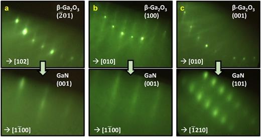
FIG. 1. Reflection high-energy electron diffraction (RHEED) patterns of the transformation of (a)(-201), (b) (100), and (c) (001) BGO to GaN. In (a) and (b) c-plane GaN symmetry is observed, while (101) GaN symmetry is observed in (c).
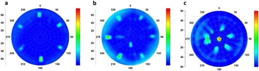
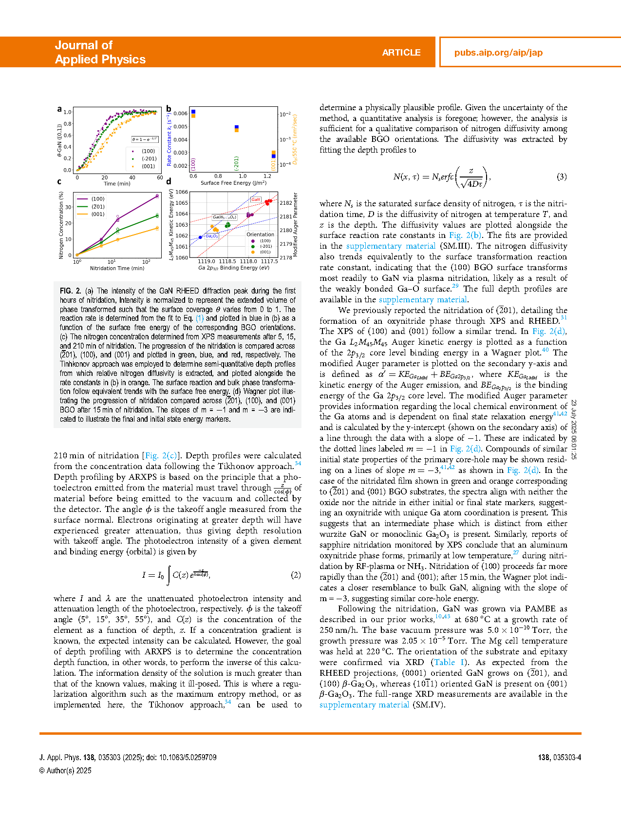
FIG. 2. XRD pole figures of the GaN 202 reflection on BGO (-201) (a), and BGO (100) (b), and of the GaN 100 reflection on BGO (001) (c). In (c), the BGO zone axis is present at the center as the 2θ of the symmetric BGO 002 overlaps the asymetric GaN 100 reflection. No duplicate or shifted peaks were observed, indicating a cohesive single crystal GaN epitaxy.
DOI:
doi.org/10.1063/5.0259709