Paper Sharing
【Member Papers】Proposal and Simulation of β-Ga₂O₃ Hetero-Junction Schottky Diodes With Low Work-Function Anode and High Breakdown Voltage
日期:2025-08-08阅读:521
Researchers from the Xidian University have published a dissertation titled "Proposal and Simulation of β-Ga2O3 Hetero- Junction Schottky Diodes With Low Work-Function Anode and High Breakdown Voltage" in IEEE Journal of the Electron Devices Society.
Background
β-Ga2O3 is an attractive semiconductor material for high power and high frequency electronic applications due to its unique material properties, such as high critical electric field (Ec) of ~8 MV/cm from its ultra-wide bandgap of 4.5-4.9 eV, decent intrinsic electron mobility of ~200 cm2V-1 s-1 as well as a high electron saturation velocity of ∼2×107 cm/s, which gives Ga2O3 a theoretical Baliga’s figure-of-merit (BFOM) and Johnson’s figure-of-merit (JFOM) to be several times higher than that of SiC and GaN. In addition to these superior material properties, β-Ga2O3 is advantageous when it comes to material growth methodologies. β-Ga2O3 bulk single crystal can be grown by melt-grown methods, which allows for the production of low-cost, large-size, and high-quality commercial compatible substrates. This also enables high-quality homoepitaxy and reveals the enormous potential of β-Ga2O3 for future wide spread high-power applications.
Abstract
In this work, we propose a p-NiO/n-Ga2O3 hetero-junction (HJ) Schottky barrier diode (SBD) with low turn-on voltage (Von) and high breakdown voltage (BV) with a trench SBD as a control. An investigation of its electrical characteristics is simulated by Sentaurus TCAD. The HJ SBD utilizes a low work-function anode metal to form a top electrode by reducing the Von of the diode at the forward state. A fin structure and metal/semiconductor (M/S) junction or PN HJ was employed to achieve an enhanced BV at the reverse state. An attempt to optimize the electrical characteristics of the device by modifying its structural parameters is also comprehensively analyzed in this work. The HJ SBD achieves a low Von of 0.57 V and a Power Figure of Merit (P-FOM) of 3.79 GW/cm2, simultaneously. The proposed structure provides a new approach for realizing high performance β-Ga2O3 SBDs with high reverse blocking and low loss capabilities.
Conclusion
In summary, p-NiO/n-Ga2O3 HJ SBD structures with low Von and high BV were proposed and investigated by Sentaurus TCAD simulations. This work has systematically studied the effect of the device Von reduction strategies without significantly sacrificing the BV. This is done by changing the work-function of top anode and using Schottky contacts or HJs with fin structure to assist the fin side-wall depletion. Through the optimization of device parameters, a typical Von of 0.57 V and P-FOM of 3.79 GW/cm2 was simulated for the HJ SBD with an RHW of 0.12, WFin of 5 μ m, WSpace of 3 μm, a TNiO of 300 nm, and a top metal SBH of 0.9 eV. References indicate that Schottky contacts formed with metals like Ti and Mo in conjunction with β-Ga2O3 exhibit a Schottky Barrier Height close to our projected value. Additionally, future advancements in surface treatment could potentially reduce the SBH of the M/S contact, aligning it with our anticipated targets. Consequently, it is believed that the structure outlined in this article is capable of achieving the dual objectives of low Von and high BV for future high power and low loss applications.
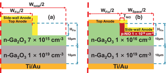
FIGURE 1. Schematic cross-section image of the (a) trench SBD and (b) p-NiO/n-Ga2O3 HJ SBD with low work-function anode on the fin top.
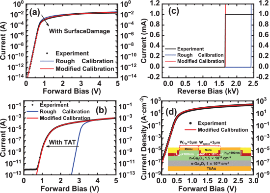
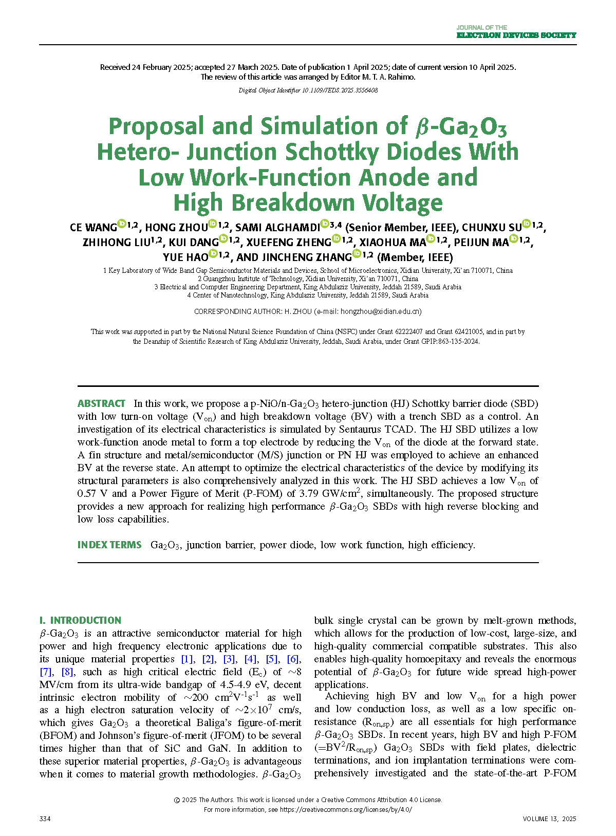
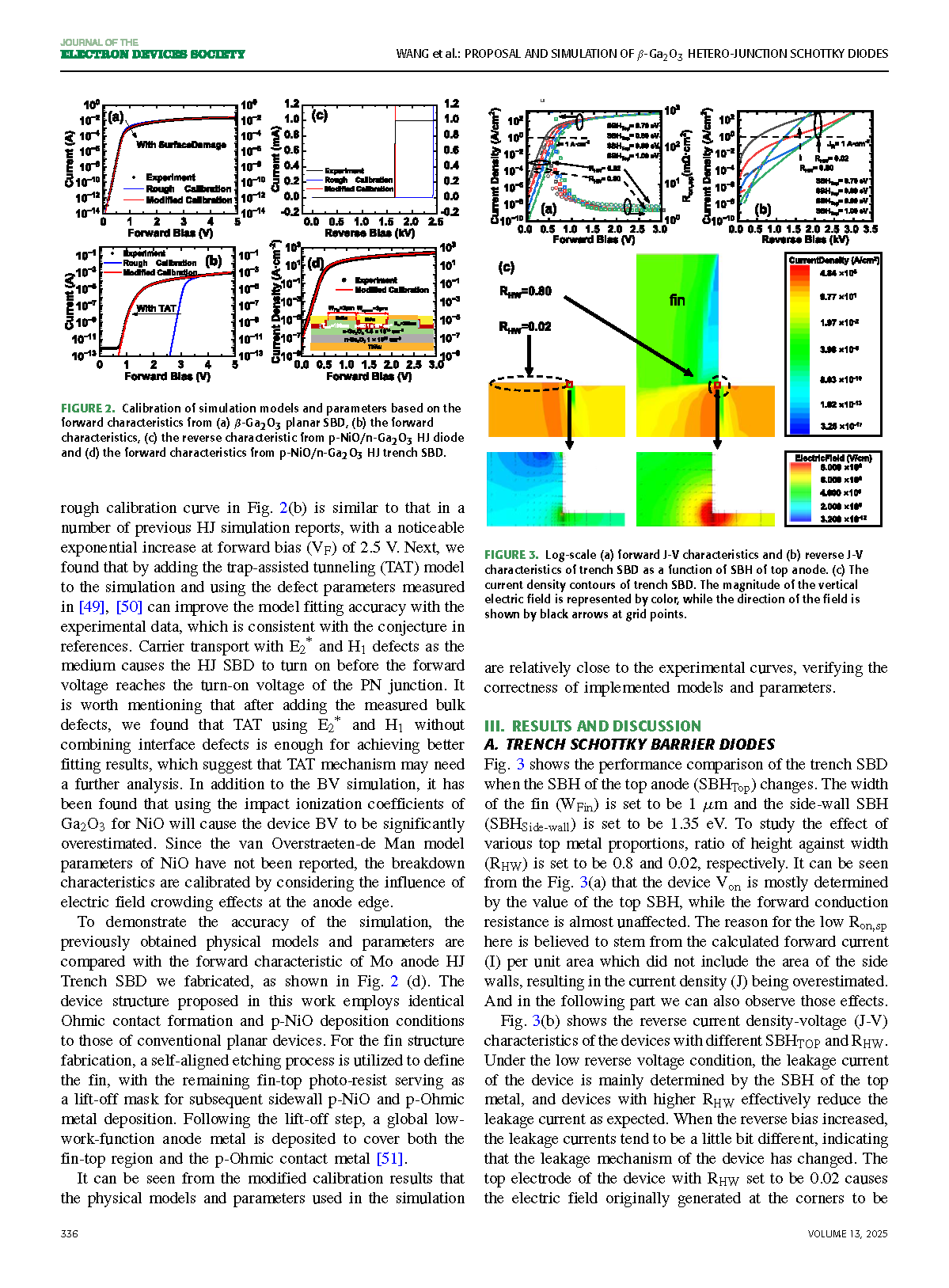
FIGURE 2. Calibration of simulation models and parameters based on the forward characteristics from (a) β -Ga2O3 planar SBD, (b) the forward characteristics, (c) the reverse characteristic from p-NiO/n-Ga2O3 HJ diode and (d) the forward characteristics from p-NiO/n-Ga2O3 HJ trench SBD.
DOI:
doi.org/10.1109/JEDS.2025.3556408