Paper Sharing
【International Papers】Optical and Structural Characterization of Cu-Doped Ga₂O₃ Nanostructures Synthesized via Hydrothermal Method
日期:2025-08-07阅读:555
Researchers from the Korea Aerospace University have published a dissertation titled "Optical and Structural Characterization of Cu-Doped Ga2O3 Nanostructures Synthesized via Hydrothermal Method" in Inorganics.
Background
Gallium oxide (Ga2O3), a wide-bandgap semiconductor with a bandgap of approximately 4.9 eV, has attracted significant attention for its potential applications in optoelectronic devices, power electronics, and deep ultraviolet photodetectors due to its high breakdown voltage, chemical stability, and transparency to UV light. Among the various polymorphs of Ga2O3, the monoclinic β-phase is the most thermodynamically stable at ambient conditions, making it particularly suitable for high-temperature and high-power applications. The introduction of various dopants into β-Ga2O3 is a well-established strategy for effectively modulating its electrical, optical, and structural properties.
Abstract
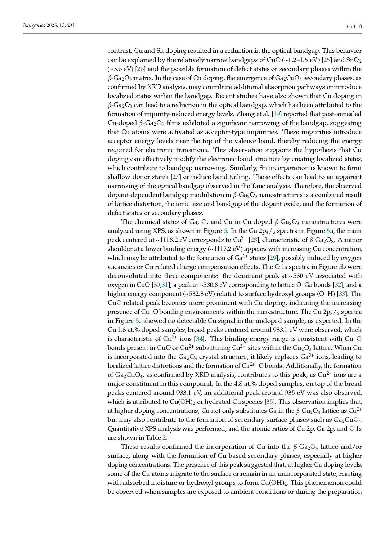
In this study, we investigate the optical and structural properties of Cu-doped β-Ga2O3 nanostructures synthesized via a hydrothermal method, followed by annealing in ambient O2. Different Cu doping concentrations (0, 1.6, and 4.8 at.%) are introduced to examine their effects on the crystal structure, chemical state, and optical bandgap of β-Ga2O3. X-ray diffraction (XRD) analysis reveals that the host β-Ga2O3 crystal structure is preserved at lower doping levels, whereas secondary phases (Ga2CuO4) appear at higher doping concentrations (4.8 at.%). X-ray photoelectron spectroscopy (XPS) confirms the presence of Cu2+ ions in both lattice substitution sites and surface-adsorbed hydroxylated species (Cu(OH)2). The optical bandgap of β-Ga2O3 is found to decrease with increasing Cu concentration, likely due to the formation of localized states or secondary phases. These findings demonstrate the tunability of the optical properties of β-Ga2O3 via Cu doping, providing insights into the incorporation mechanisms and their impact on structural and electronic properties.
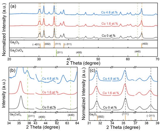
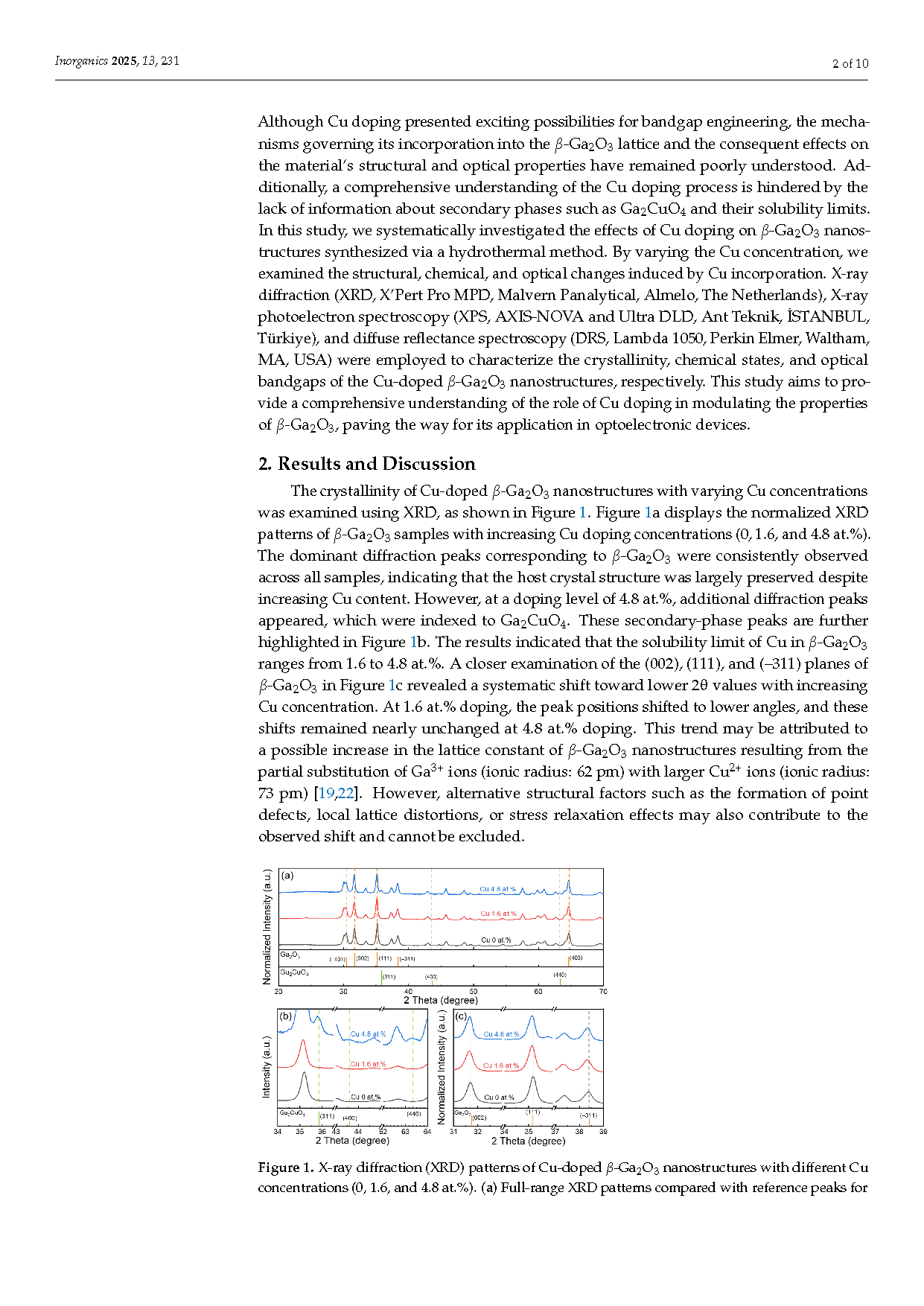
Figure 1. X-ray diffraction (XRD) patterns of Cu-doped β-Ga2O3 nanostructures with different Cu concentrations (0, 1.6, and 4.8 at.%). (a) Full-range XRD patterns compared with reference peaks for β-Ga2O3 and Ga2CuO4. (b) Magnified view of selected diffraction regions highlighting the (311), (400), and (440) planes of Ga2CuO4. (c) Enlarged view of the (002), (111), and (–311) planes of β-Ga2O3, showing a progressive shift in the main peaks toward lower 2θ values with increasing Cu content.
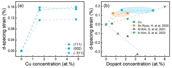
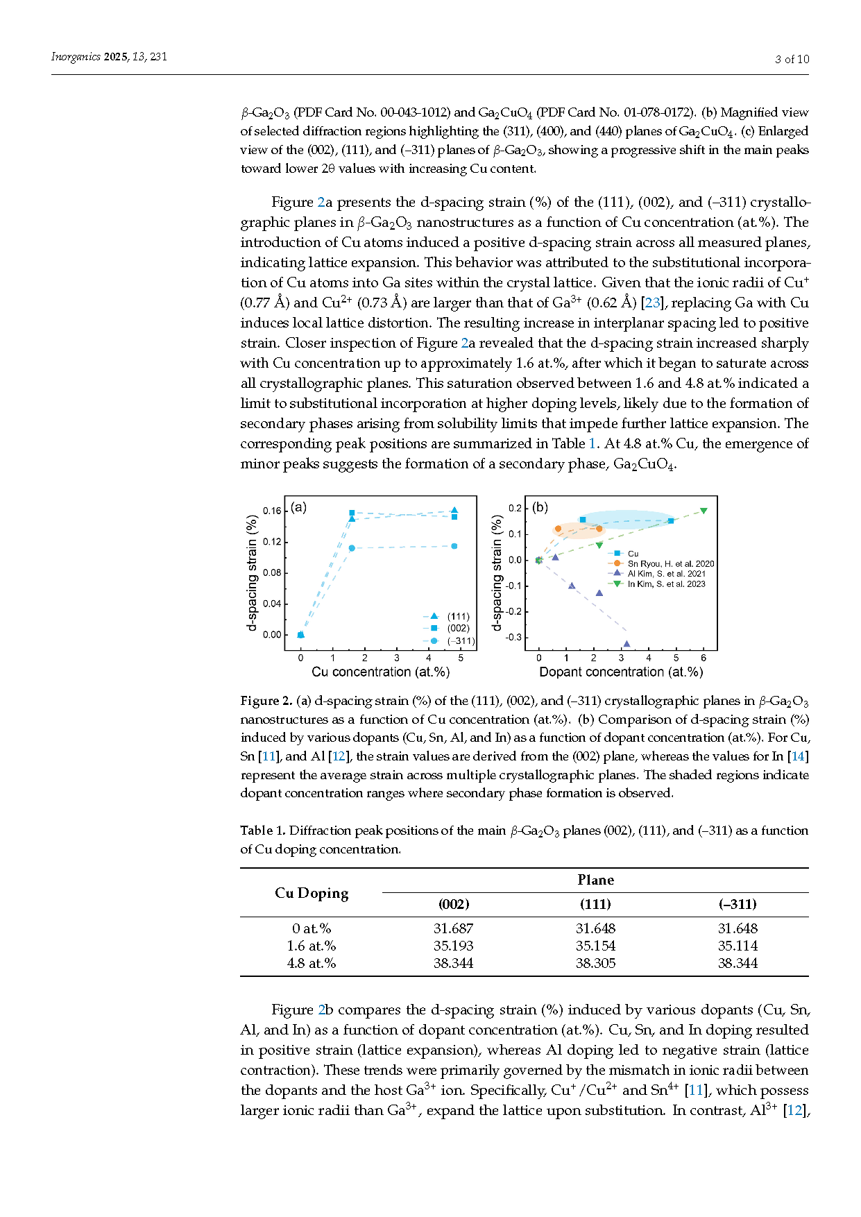
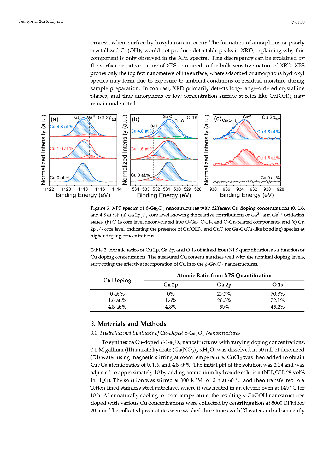
Figure 2. (a) d-spacing strain (%) of the (111), (002), and (–311) crystallographic planes in β-Ga2O3 nanostructures as a function of Cu concentration (at.%). (b) Comparison of d-spacing strain (%) induced by various dopants (Cu, Sn, Al, and In) as a function of dopant concentration (at.%). For Cu, Sn, and Al the strain values are derived from the (002) plane, whereas the values for In represent the average strain across multiple crystallographic planes. The shaded regions indicate dopant concentration ranges where secondary phase formation is observed.
DOI:
doi.org/10.3390/inorganics13070231