Paper Sharing
【International Papers】Assessment of Trapping Phenomena in As-Grown and Thermally-Treated Si-Doped κ-Ga₂O₃ Layers via Optical Admittance Spectroscopy
日期:2025-07-31阅读:535
Researchers from the University of Parma have published a dissertation titled "Assessment of Trapping Phenomena in As-Grown and Thermally-Treated Si-Doped κ-Ga2O3 Layers via Optical Admittance Spectroscopy" in Advanced Electronic Materials.
Background
Gallium oxide (Ga2O3) is an ultra-wide bandgap semiconductor that emerged as a promising functional material in a wide range of applications, from high-power and high-frequency electronics to deep-UV detection. Many figures of merit regarding the device performance scale non-linearly with bandgap, which puts Ga2O3 in a prominent position compared to the wide-bandgap semiconductors (WBGs). This sesquioxide possesses some appealing properties, including a high breakdown field, large Baliga's figure of merit, high switching rate, low on-resistance, controllable n-type doping, and availability of native wafers from the melt growth technique. Five different polymorphs of this material system are known: α, β, γ, δ, κ (previously denoted as ɛ). The monoclinic β-Ga2O3 is the thermodynamically stable phase, which received more attention than other polymorphs. Nonetheless, this polymorph suffers from low structural symmetry associated with the monoclinic crystal structure and a strong tendency to cleavage along the (100) and (001) planes.
Abstract
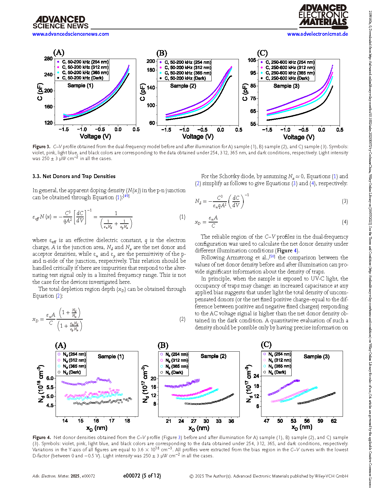
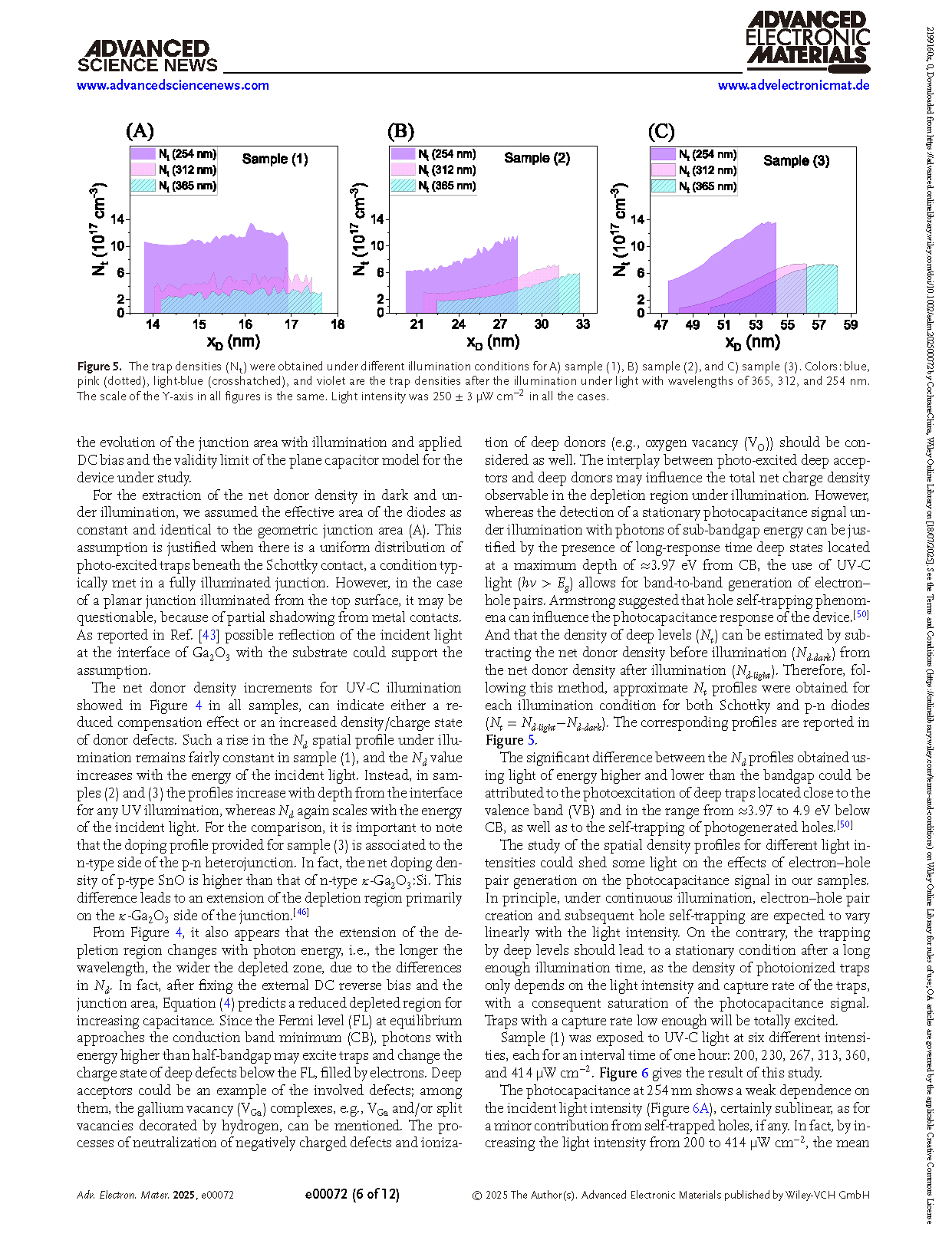
The impact of thermal treatments on the trapping phenomena in (001) Si-doped κ-Ga2O3 epi-layers, via optical admittance spectroscopy technique, is reported. Two Pt/κ-Ga2O3 Schottky contacts are investigated: one made on top of an as-grown Si-doped κ-Ga2O3 layer and the other on a thermally treated one. Three different illumination conditions, including monochromatic UV-C (λ = 254 nm), UV-B (λ = 312 nm), and UV-A (λ = 365 nm), are employed for the capacitance–voltage (C–V) measurements at different bias and AC frequencies to investigate traps and deep levels in κ-Ga2O3:Si. The net donor density profiles in dark and approximate density of photoionized traps of the as-grown and thermally treated samples are extracted from the C–V curves in the dual-frequency mode under different illumination conditions. A SnO/κ-Ga2O3 p-n heterojunction, where the κ-Ga2O3:Si layer underwent a double thermal treatment, is also investigated to better understand the relation between thermal treatment and distribution of trap density. The transient photocapacitance and photocurrent measurements are performed under the same illumination conditions to evaluate the response times of traps. This study provides a better understanding of the trapping phenomena in the as-grown and thermally treated κ-Ga2O3:Si epi-layers, which are important for UV-C detection applications.
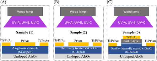
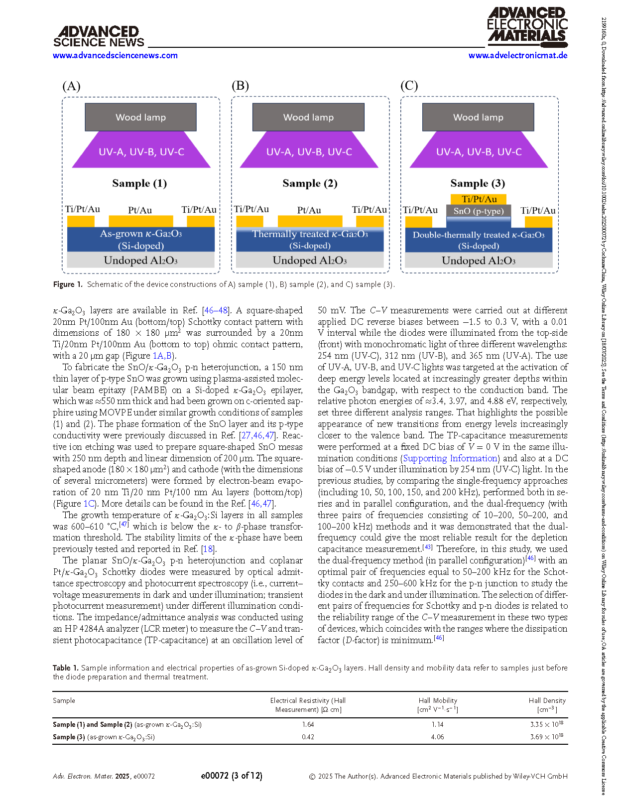
Figure 1. Schematic of the device constructions of A) sample (1), B) sample (2), and C) sample (3).
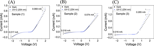
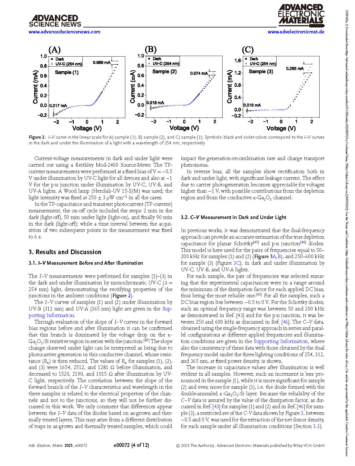
Figure 2. I–V curve in the linear scale for A) sample (1), B) sample (2), and C) sample (3). Symbols: black and violet colors correspond to the I–V curves in the dark and under the illumination of a light with a wavelength of 254 nm, respectively.
DOI:
doi.org/10.1002/aelm.202500072