Paper Sharing
【Domestic Papers】Source-Field-Plated β-(AlₓGa₁₋ₓ)₂O₃ MOSFET with Breakdown Voltage Over 7kV
日期:2025-07-28阅读:549
Researchers from the Hebei Semiconductor Research Institute and University of Science and Technology of China have published a dissertation titled "Source-Field-Plated β-(AlxGa1-x)2O3 MOSFET with Breakdown Voltage Over 7kV" in Micro and Nanostructures.
Project Support
This work was supported by the National Key Research and Development Program of China under Grant 2024YFE0205300.
Background
Beta-Ga2O3, an ultra-wide bandgap (UWBG) semiconductor, has emerged as a promising candidate for next-generation power electronics due to its high critical electric field (∼8 MV/cm) and Baliga figure of merit (BFOM) surpassing conventional materials like SiC and GaN [1,2]. However, the relatively low thermal conductivity and limited bandgap tunability of pure β-Ga2O3 restrict its performance in high-power and high-frequency applications. To address these limitations, β-(AlxGa1-x)2O3/β-Ga2O3 heterostructures have been extensively explored, leveraging the alloying of Al2O3 with β-Ga2O3 to achieve tunable bandgaps (4.8–6.2 eV for Al content x = 0–0.71), enhanced BFOM [[3], [4], [5], [6]] and higer thermal conductivity (up to 30.4 W cm−1 K−1) [7]. These heterostructures enable superior electrostatic control and carrier confinement, making them ideal for high-electron-mobility transistors (HEMTs) and other power devices.
Abstract
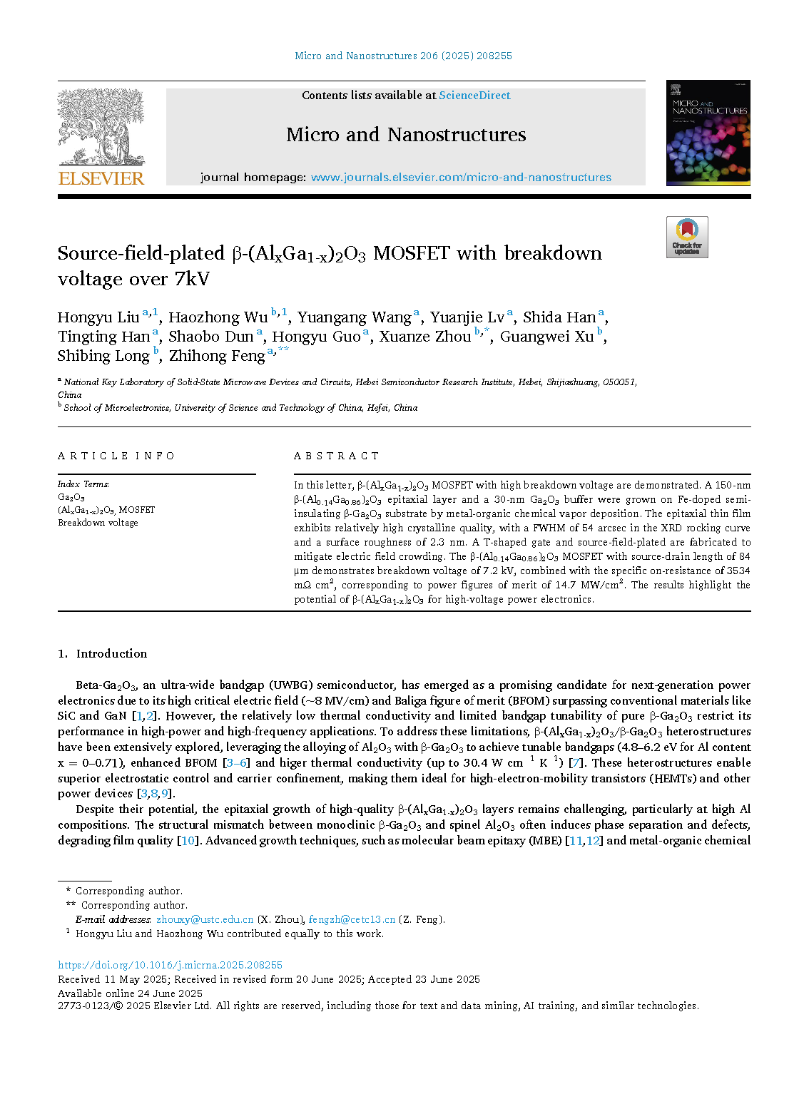
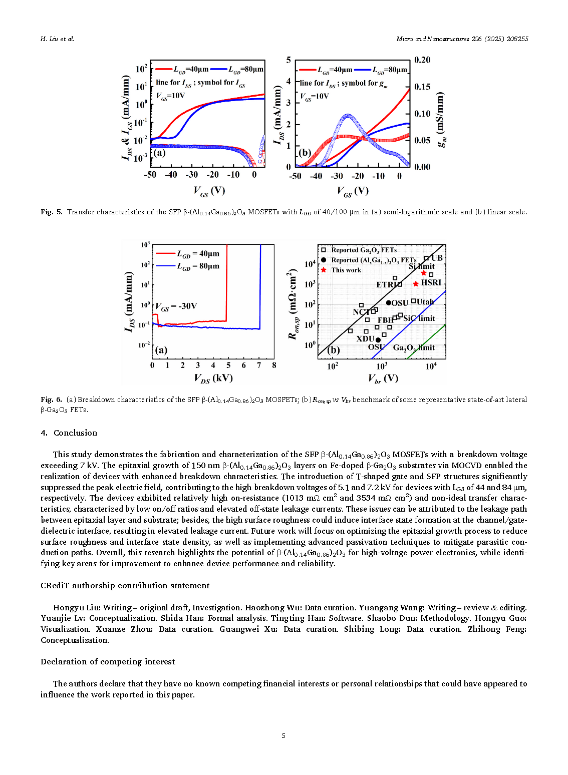
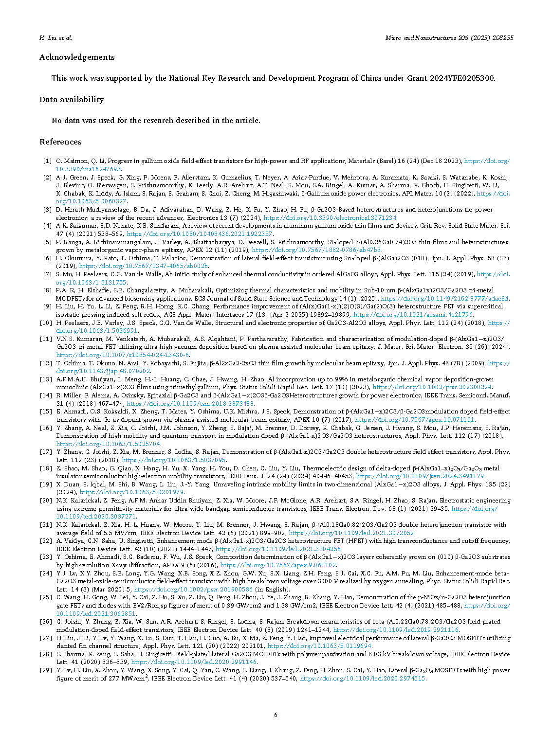
In this letter, β-(AlxGa1-x)2O3 MOSFET with high breakdown voltage are demonstrated. A 150-nm β-(Al0.14Ga0.86)2O3 epitaxial layer and a 30-nm Ga2O3 buffer were grown on Fe-doped semi-insulating β-Ga2O3 substrate by metal-organic chemical vapor deposition. The epitaxial thin film exhibits relatively high crystalline quality, with a FWHM of 54 arcsec in the XRD rocking curve and a surface roughness of 2.3 nm. A T-shaped gate and source-field-plated are fabricated to mitigate electric field crowding. The β-(Al0.14Ga0.86)2O3 MOSFET with source-drain length of 84 μm demonstrates breakdown voltage of 7.2 kV, combined with the specific on-resistance of 3534 mΩ cm2, corresponding to power figures of merit of 14.7 MW/cm2. The results highlight the potential of β-(AlxGa1-x)2O3 for high-voltage power electronics.
Highlights
● Addressed challenges in epitaxial growth, achieving 150 nm β-(Al0.14Ga0.86)2O3 layers.
● Implemented T-shaped gate and source-field-plated structures to enhance performance.
● Achieved 7.2 kV breakdown voltage in β-(Al0.13Ga0.87)2O3 MOSFETs.
● Demonstrated power figure of merit up to 14.7 MW/cm2 for high-voltage applications.
Conclusion
This study demonstrates the fabrication and characterization of the SFP β-(Al0.14Ga0.86)2O3 MOSFETs with a breakdown voltage exceeding 7 kV. The epitaxial growth of 150 nm β-(Al0.14Ga0.86)2O3 layers on Fe-doped β-Ga2O3 substrates via MOCVD enabled the realization of devices with enhanced breakdown characteristics. The introduction of T-shaped gate and SFP structures significantly suppressed the peak electric field, contributing to the high breakdown voltages of 5.1 and 7.2 kV for devices with LGS of 44 and 84 μm, respectively. The devices exhibited relatively high on-resistance (1013 mΩ cm2 and 3534 mΩ cm2) and non-ideal transfer characteristics, characterized by low on/off ratios and elevated off-state leakage currents. These issues can be attributed to the leakage path between epitaxial layer and substrate; besides, the high surface roughness could induce interface state formation at the channel/gate-dielectric interface, resulting in elevated leakage current. Future work will focus on optimizing the epitaxial growth process to reduce surface roughness and interface state density, as well as implementing advanced passivation techniques to mitigate parasitic conduction paths. Overall, this research highlights the potential of β-(Al0.14Ga0.86)2O3 for high-voltage power electronics, while identifying key areas for improvement to enhance device performance and reliability.
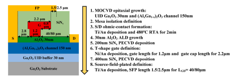
Fig. 1. The cross-section schematic of the SFP β-(Al0.14Ga0.86)2O3 MOSFETs and its fabrication details.
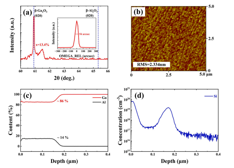
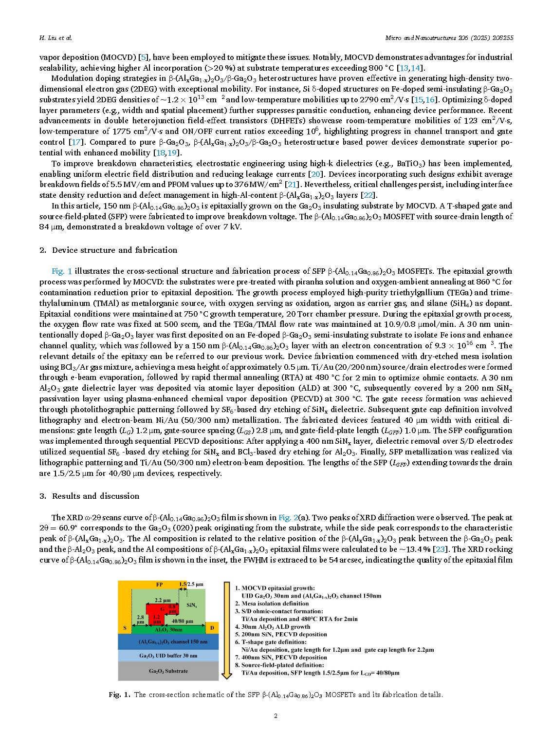
Fig. 2. (a) XRD ω-2θ scans and rocking curve, (b) AFM image of the β-(Al0.14Ga0.86)2O3 film, (c) SIMS of Al/Ga content and (d) Si distribution depth profiles of the β-(Al0.14Ga0.86)2O3 film.
DOI:
doi.org/10.1016/j.micrna.2025.208255