Paper Sharing
【International Papers】Thickness dependence of optoelectronic properties of gallium oxide film deposited by electron beam evaporation technique
日期:2025-07-24阅读:604
Researchers from the University Sains Malaysia have published a dissertation titled "Thickness dependence of optoelectronic properties of gallium oxide film deposited by electron beam evaporation technique" in Optical and Quantum Electronics.
Background
Gallium oxide (Ga2O3) has consistently captured the interest of researchers since its discovery in the 1950s, owing to its distinctive intrinsic physical properties. It is characterized by an ultra-wide bandgap (Eg), and a remarkable breakdown field. The β-Ga2O3 crystal structure is recognized as the most stable form of Ga2O3 and qualifies as a wide-bandgap semiconductor, with a bandgap of approximately 4.8 eV. Additionally, it exhibits a high breakdown electric field, estimated at around 8 MV/cm, deep-UV (< 300 nm) transparency, strong radiation, medium dielectric constant, and high-temperature stability. Also, it is used in manufacturing of power electronics' high-voltage field-effect transistors (MOSFET, FET). Consequently, it boasts a Baliga's figure of merit that is roughly 10 times greater than that of 4H-SiC and about 200 times higher than that of GaAs. Due to the promising properties mentioned above, Ga2O3 is employed in different applications such as transparent conducting oxide, gas sensing, antireflection coating, solar blind UV photodetector, metal–oxide–semiconductor capacitors, photoelectrochemical water splitting.
Abstract
In this study, the effects of β-Ga2O3 film thickness on morphological, topological, compositional, structural, optical, and optoelectronic properties were examined. The films were deposited onto sapphire and quartz substrates using electron beam evaporation. The surface roughness of the films was analyzed using atomic force microscopy, showing an increase from 2.70 nm to 5.03 nm as the film thickness increased. The grain size transitioned from sparse, tiny grains to a more uniform distribution of slightly larger grains, as revealed by field emission scanning electron microscopy. The presence of gallium and oxygen atoms was confirmed through energy-dispersive X-ray spectroscopy. The films showed β-Ga2O3 polycrystalline structures as confirmed by X-ray diffraction analysis. The inter-planar spacing and crystallite size increased from 6.67 to 10.74 nm as film thickness increased. In contrast, the energy band gap decreased from 5.12 eV to 4.87 eV. The optical density, skin depth, optical sheet resistance, and thermal emissivity were in the order of 0–3, 102 cm, 10–7 Ωm2, and 10–12, respectively. The study also revealed that the optoelectronic parameters such as optical density, refractive index, packing density, dispersive energy, single oscillator energy, charge carrier concentration, plasma frequency, relaxation time, optical conductivity and resistivity increased with the thickness of the films. In contrast, other parameters such as skin depth, absorption coefficient, extinction coefficient, band gap energy, porosity, lattice dielectric constant, optical sheet resistance, and thermal emissivity decreased as the film thickness increased.
Conclusions
Polycrystalline β-Ga₂O₃ thin films were successfully deposited at room temperature using electron beam evaporation, and their structural, morphological, topological, optical, and optoelectronic properties were systematically studied as a function of film thickness. Surface roughness, measured via AFM, increased significantly from 2.70 nm to 5.03 nm with greater thickness, while FESEM imaging revealed the evolution of grain morphology from sparse, diminutive grains to a more uniform arrangement of larger grains, indicating enhanced grain growth. EDX spectroscopy confirmed the presence of gallium and oxygen, essential for β-Ga2O3 formation, and XRD analysis demonstrated improved crystallinity with increasing thickness and annealing. Key optoelectronic properties of the films were characterized, yielding relaxation times, carrier concentrations, plasma frequencies, optical mobilities, and resistivities on the order of 10–19 s, 1017 cm⁻3, 1010 Hz, 10–7, and 10–2 Ω·cm, respectively. Notably, increasing film thickness increased the optical density, refractive index, packing density, dispersive energy, single oscillator energy, carrier concentration, plasma frequency, relaxation time, optical conductivity, and resistivity. In contrast, parameters such as skin depth, absorption coefficient, extinction coefficient, bandgap energy, porosity, lattice dielectric constant, optical sheet resistance, and thermal emissivity decreased. These findings provide valuable insights into the tunable properties of β-Ga2O3 thin films and their potential for diverse applications in optoelectronics and electronics, including photodetectors, sensors, and power devices. Additionally, the compatibility of β-Ga₂O₃ with III-nitride technologies highlights its promise for integration in advanced device architectures.
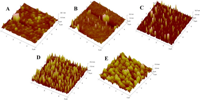
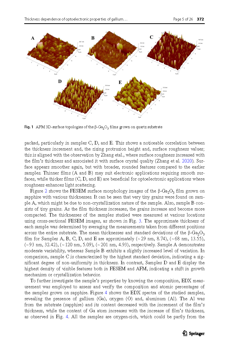
Fig. 1. AFM 3D-surface topologies of the β-Ga2O3 films grown on quartz substrate
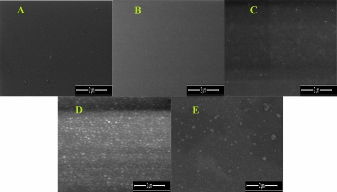
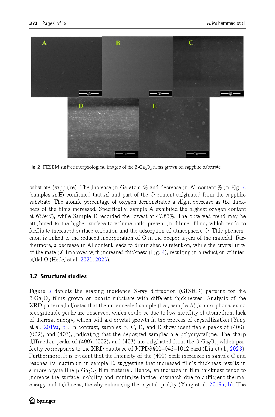
Fig. 2. FESEM surface morphological images of the β-Ga2O3 films grown on sapphire substrate
DOI:
doi.org/10.1007/s11082-025-08272-3