Paper Sharing
【International Papers】On Ga₂O₃ Self-Switching Nano-Diodes
日期:2025-07-21阅读:535
Researchers from the King Abdullah University of Science and Technology (KAUST) have published a dissertation titled "On Ga2O3 Self-Switching Nano-Diodes" in Advanced Electronic Materials.
Background
Beta-phase of Gallium Oxide (β-Ga2O3) has garnered significant attention in recent years as a potential candidate for next-generation power electronics due to its unique material properties and suitability for mass production. It possesses an ultra-wide bandgap of ≈4.8 eV, a high critical electric field of ≈8 MV cm−1, and has a scalable low-cost substrate growth functionality. Consequently, β-Ga2O3 based devices are expected to outperform their SiC and GaN counterparts for certain applications. Power diodes based on β-Ga2O3 have already surpassed the 1-D unipolar limit of SiC and GaN.
Now, diodes are an integral part of most of the power converter circuits. While some diodes are used as switches, others are used to prevent hard saturation of transistors and protection of circuits from voltage spikes. Talking about β-Ga2O3, the majority of the β-Ga2O3 diodes developed so far are predominantly Schottky barrier diodes and p-n junction diodes. Interestingly, β-Ga2O3 photodiodes are also emerging as a promising candidate for deep ultraviolet (deep-UV) photodetection.
Abstract
In this work, a Ga2O3 self-switching nano-diode (SSND) fabricated on a sapphire substrate is presented. Unlike previous SSND studies that primarily focused on rectification, this work explores additional device characteristics, including breakdown voltage and photodetection functionality. The diode exhibits increased current with the increase in the relative permittivity (κ) of the device trenches, and under UV illumination. Devices with increased κ achieve a high current density of ≈10 kA cm−2, a rectification ratio of ≈10⁴, and a specific on-resistance as low as 0.29 mΩ cm2. They also exhibit a breakdown voltage greater than 100 V, and a maximum power figure-of-merit of 35.46 MW cm−2. Moreover, under 240 nm light illumination, the diodes showed a responsivity close to 104 A W−1. These initial results demonstrate the potential of the SSNDs toward monolithic Ga2O3 circuits that are currently under extensive investigation for various applications.
Conclusion
In conclusion, this work shows the potential of β-Ga2O3 SSNDs toward providing multiple functionalities. β-Ga2O3 SSNDs exhibited a high current density of ≈10 kA cm−2 and an extremely low specific Ron,sp below 0.8 mΩ cm2, with a minimum of 0.29 mΩ cm2, comparable to state-of-the-art diodes fabricated on native β-Ga2O3 substrates. The SSNDs exhibited a VBR of ≈109 V and PFOM of 35.46 MW cm−2. Moreover, SSNDs showed photo-response to deep-UV light with responsivity close to 104 A W−1 under 240 nm light illumination at 15 V. Therefore, β-Ga2O3 SSNDs are thought to provide multiple promising functionalities in monolithically integrated future β-Ga2O3 circuits.
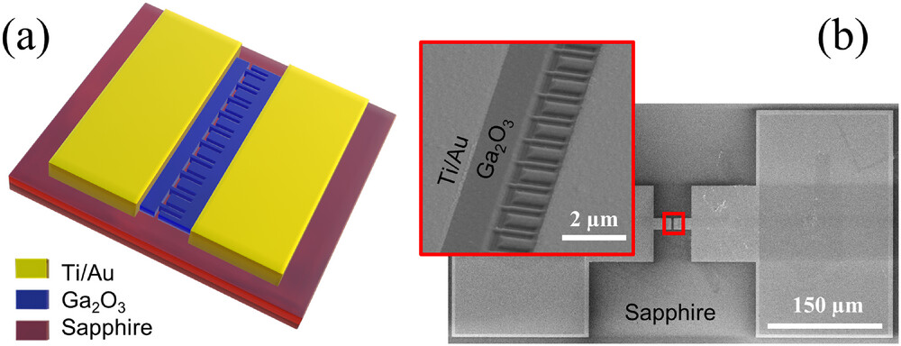
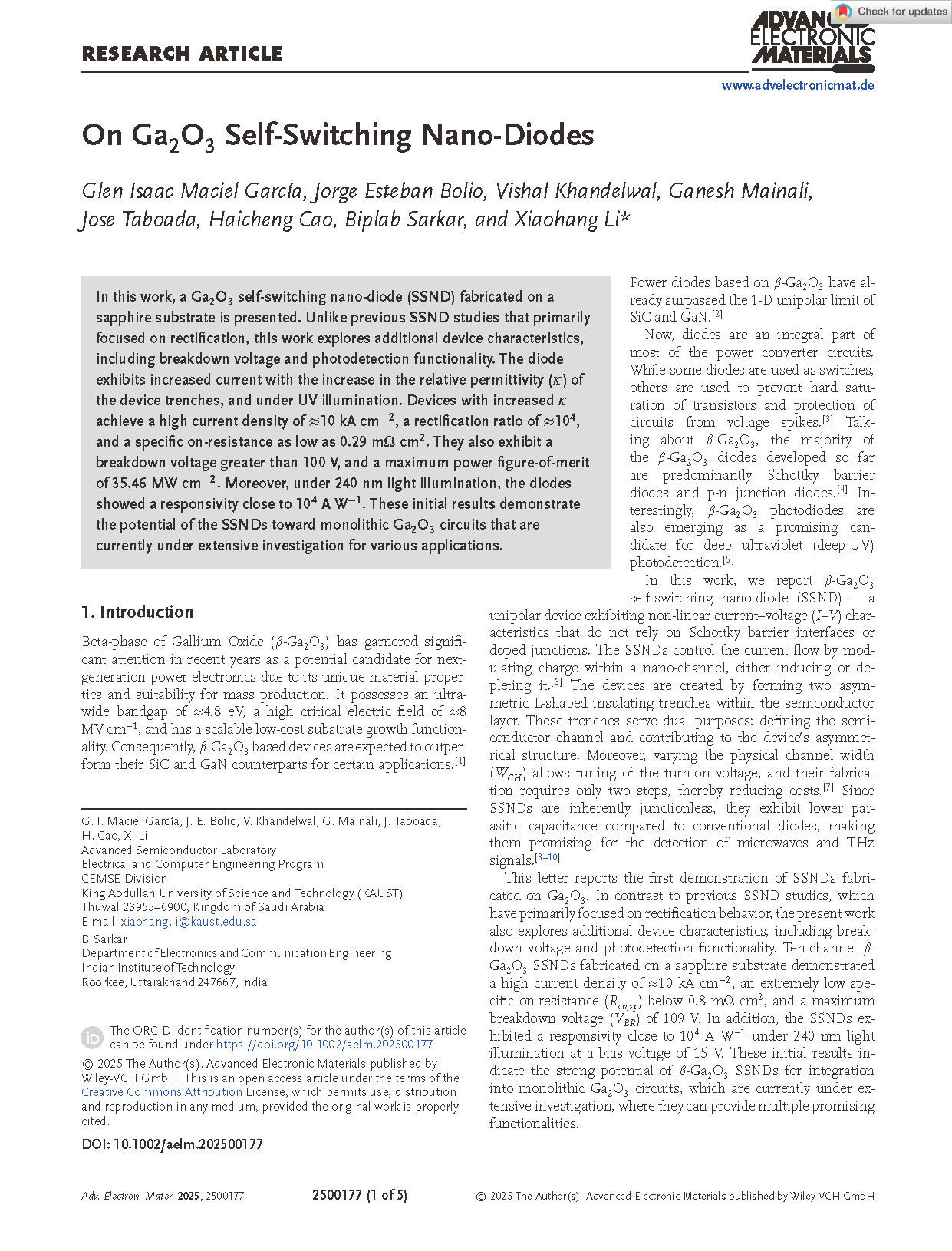
Figure 1. a) 3D Schematic view of a 10 channel Ga2O3 SSND, and b) the corresponding top view SEM image of the fabricated device.
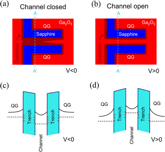
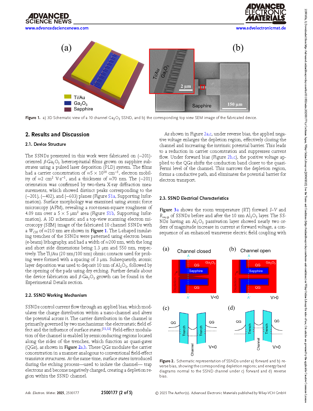
Figure 2.Schematic representation of SSNDs under a) forward and b) reverse bias, showing the corresponding depletion regions; and energy band diagrams normal to the SSND channel under c) forward and d) reverse bias.
DOI:
doi.org/10.1002/aelm.202500177