Paper Sharing
【Domestic Papers】Enhanced linear dynamic range and response speed in interdigital-electrode solar-blind photodetector by contact engineering
日期:2025-06-27阅读:539
Researchers from the Hubei University have published a dissertation titled "Enhanced linear dynamic range and response speed in interdigital-electrode solar-blind photodetector by contact engineering" in Applied Physics Reviews.
Project Support
This work was supported by the Major Program of Hubei Province under Grant No. 2023BAA009, the National Natural Science Foundation of China (Grant No. 22105162), and the Natural Science Foundation of Hubei Province (Grant No. 2023AFB623).
Background
Solar-blind ultraviolet (SBUV) photodetectors play an important role in military and civilian fields such as environmental monitoring, missile tracking, flame alarm, security communication, and oil pollution detection. As an ultra-wide bandgap (UWBG) semiconductor (Eg~4.9 eV), Ga2O3 has been used to make a variety of electronic devices, including ultraviolet detectors, field-effect transistors, Schottky diodes, and power devices. In addition, Ga2O3 has a high absorption coefficient for SBUV light, high environmental stability, high breakdown electric field strength (7–8MV/cm), and low cost. Among them, β-Ga2O3 is the most stable phase, and the other phases are metastable phases, which can be converted into b phases under certain conditions. The large-scale preparation of high quality thin films is the basis for the commercialization of Ga2O3. In recent years, much work has been done on the growth of Ga2O3 films, such as chemical vapor deposition (CVD), atomic layer deposition (ALD), pulsed laser deposition (PLD), metal-organic chemical vapor deposition (MOCVD), magnetron sputtering and molecular beam epitaxy (MBE). Among these methods, MOCVD is the preferred method for industrialization, which can achieve wafer-scale single-crystal quality of β-Ga2O3 films.
Abstract
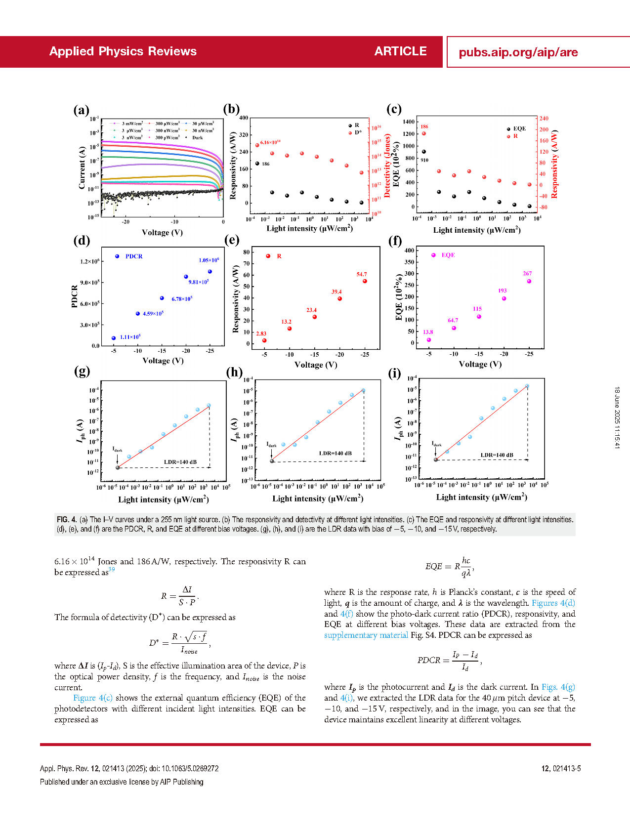
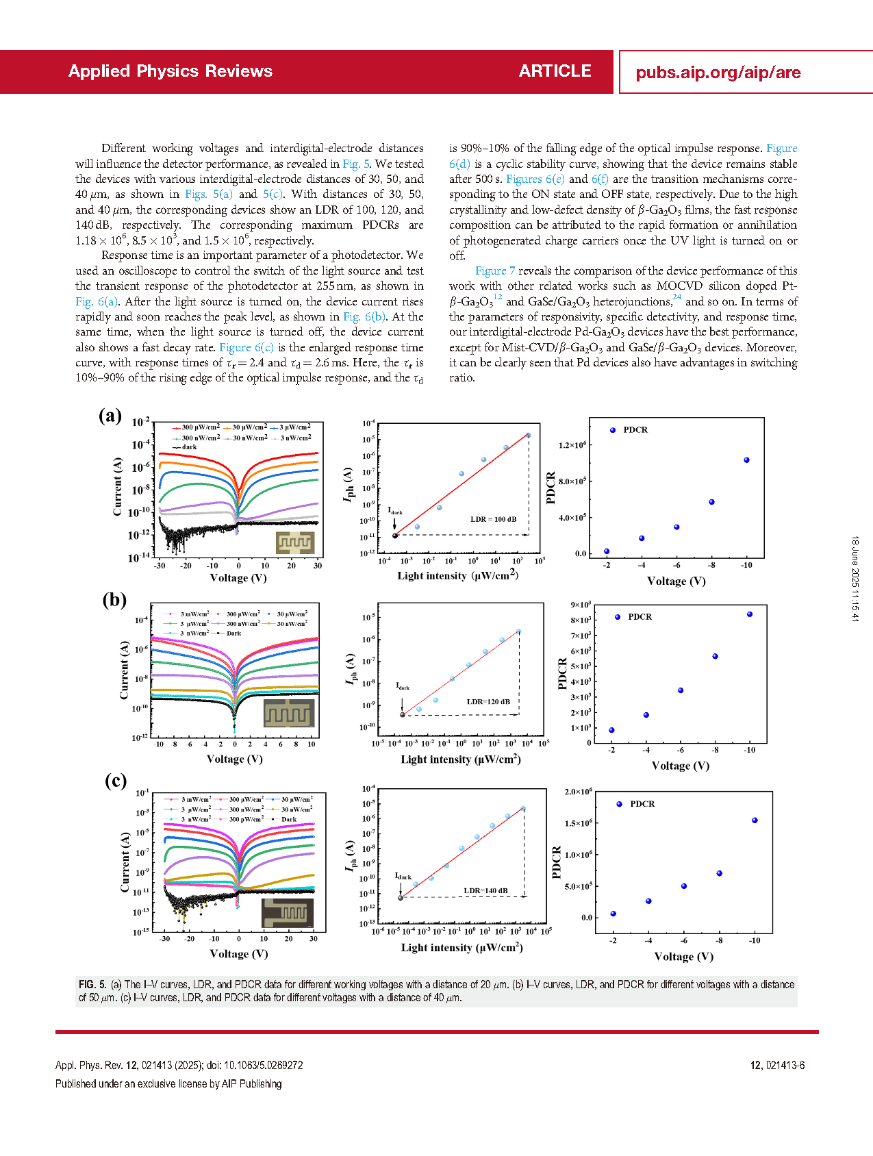
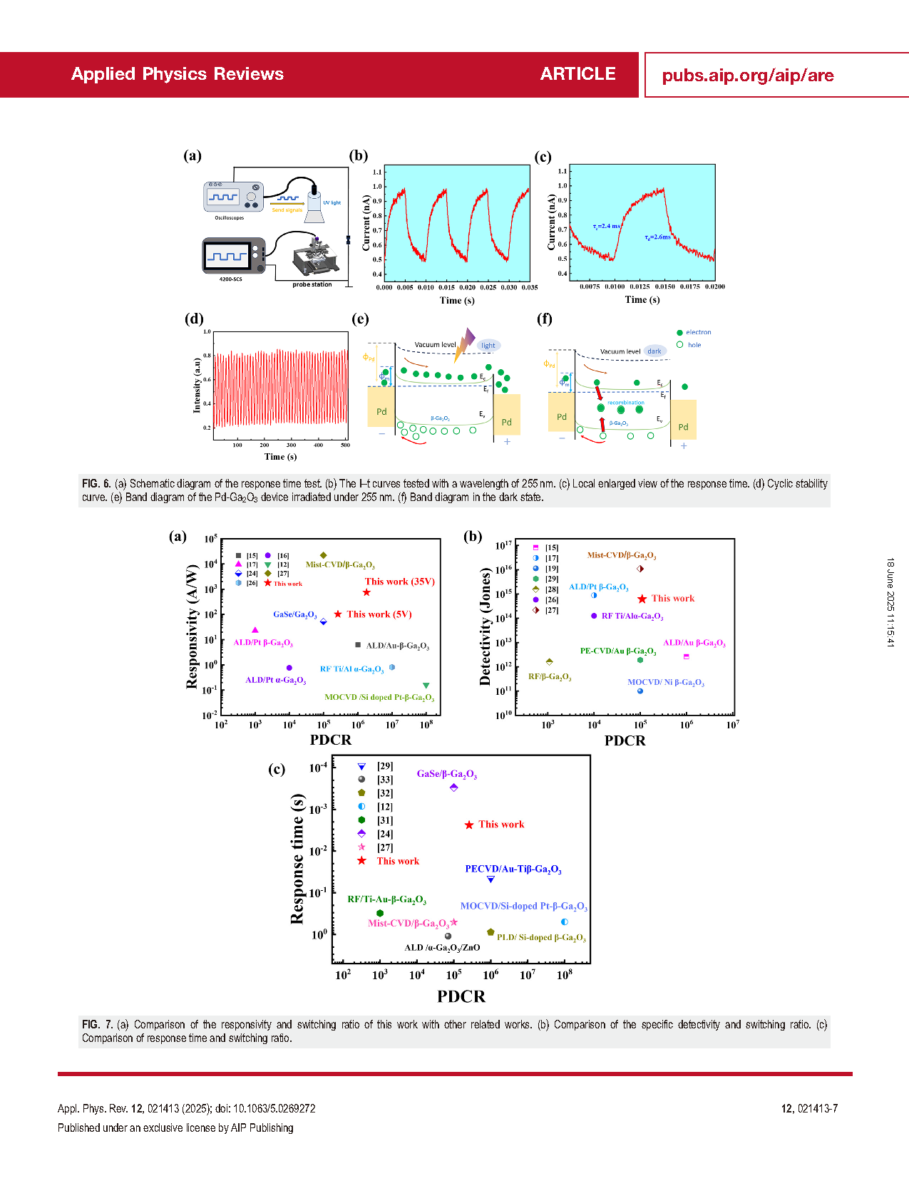
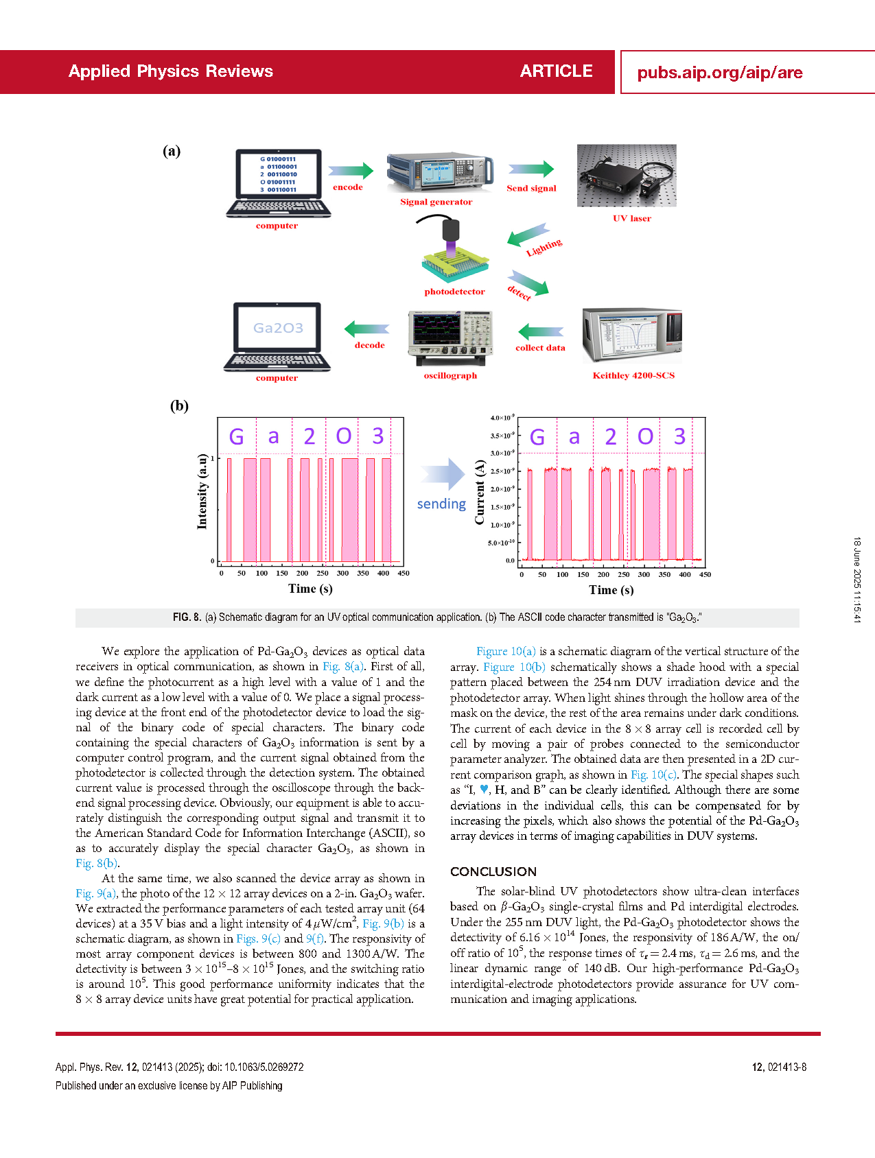
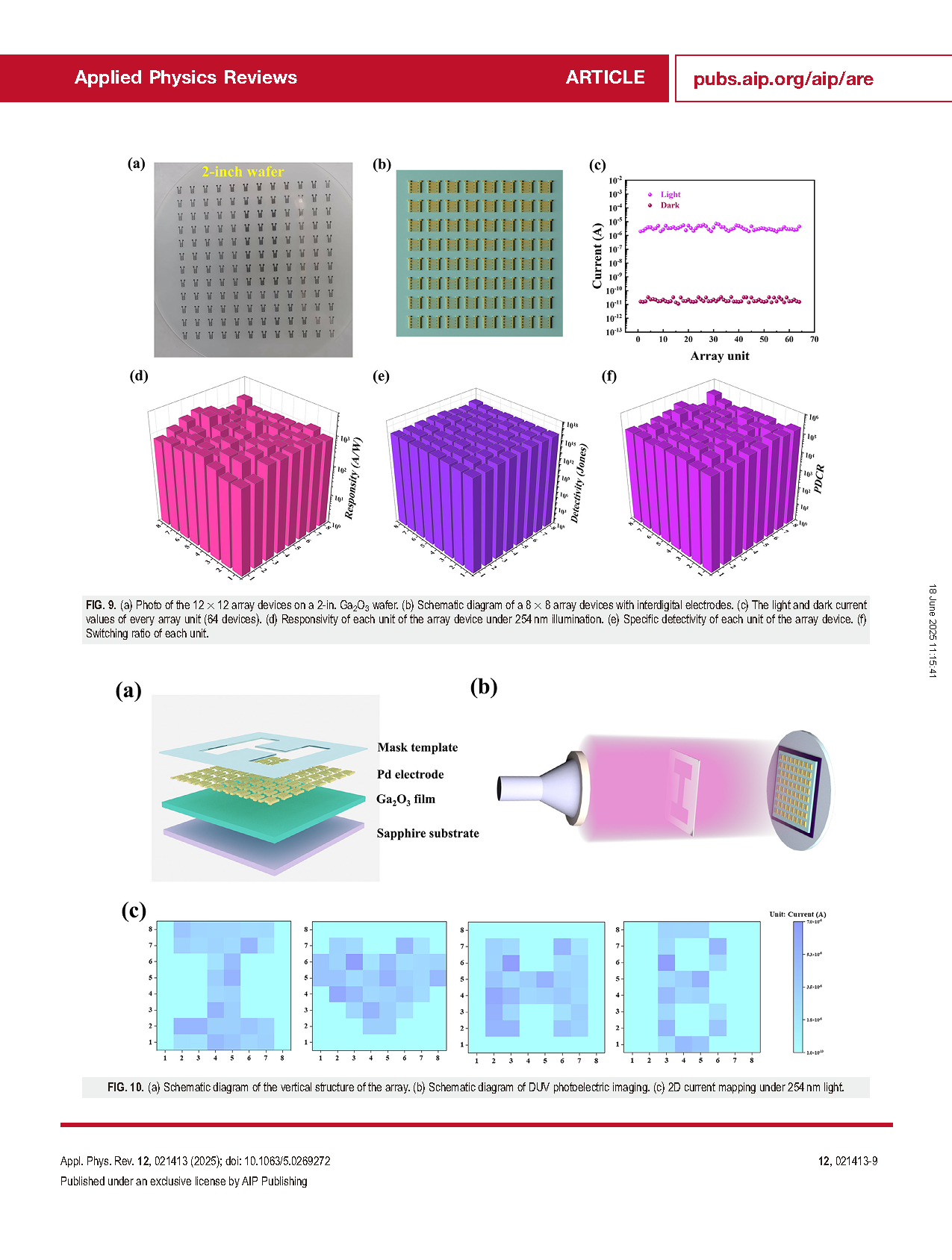
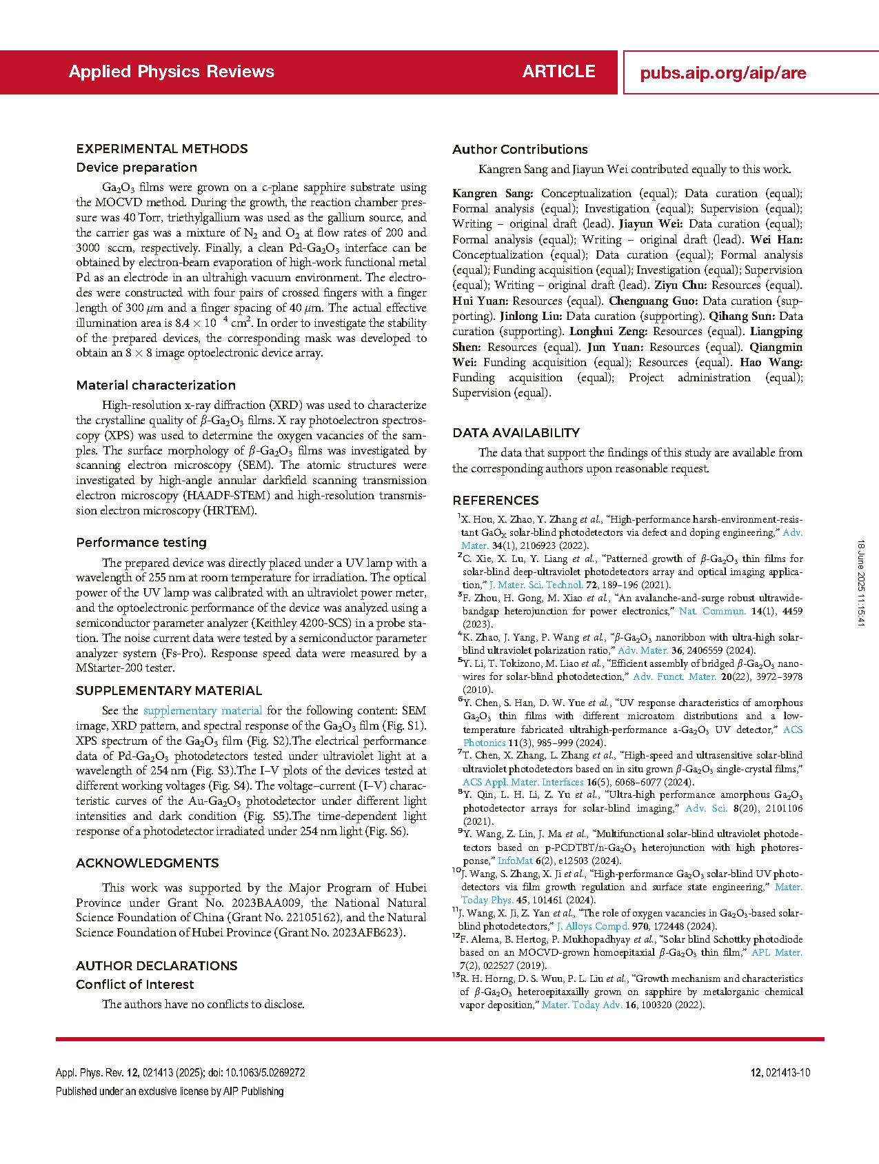
As an ultra-wide bandgap semiconductor, gallium oxide (Ga2O3) has great market potential in the field of solar-blind UV photodetectors. However, the slow response time of hundreds of milliseconds has seriously hindered the commercialization of the Ga2O3 photodetector. Here, we design an interdigital-electrode solar-blind UV β-Ga2O3 photodetector by using high-work function metal Pd as contacts. The atomic transmission electron microscopy data reveal that the Pd-Ga2O3 interface is clean and smooth, composed of a Ga2O3 single crystal and a local Pd single crystal, beneficial for weakening Fermi-level pinning. A low-damage and low-defect contact interface provides an excellent photoelectric response time of 2.4 ms (rise)/2.6 ms (descend) and a large linear dynamic range of 140 dB. On a 2-in. wafer of β-Ga2O3 film, we made a 12 × 12 array in which all 64 (8 × 8) devices tested maintained consistent performance and high reliability. Our high-performance Pd-Ga2O3 interdigital-electrode solar-blind photodetectors provide assurance for UV communication and imaging applications.
Conclusion
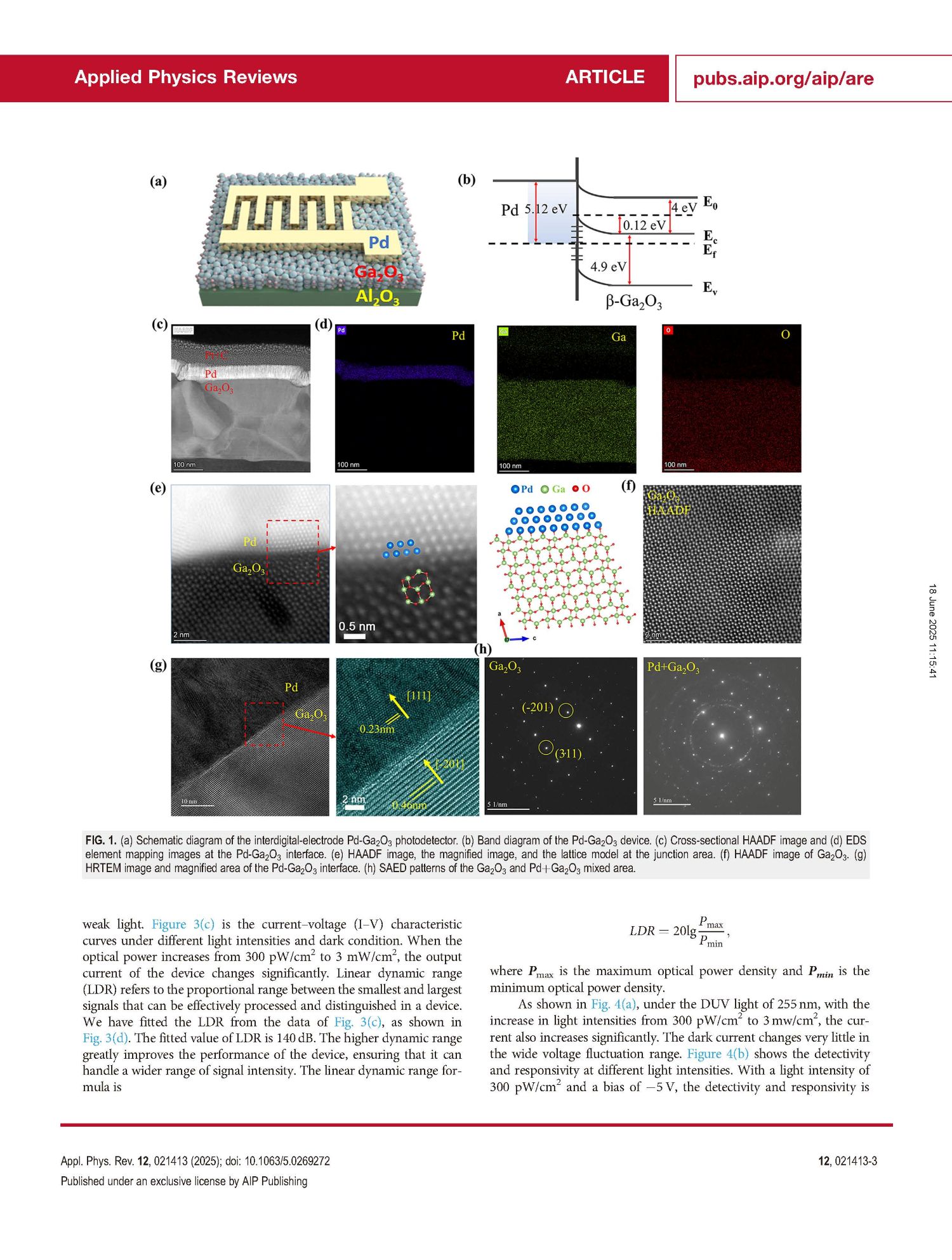
The solar-blind UV photodetectors show ultra-clean interfaces based on β-Ga2O3 single-crystal films and Pd interdigital electrodes. Under the 255 nm DUV light, the Pd-Ga2O3 photodetector shows the detectivity of 6.16×10¹⁴ Jones, the responsivity of 186A/W, the on/ off ratio of 105 , the response times of τr= 2.4 ms, τd= 2.6 ms, and the linear dynamic range of 140 dB. Our high-performance Pd-Ga2O3 interdigital-electrode photodetectors provide assurance for UV communication and imaging applications.
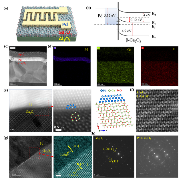
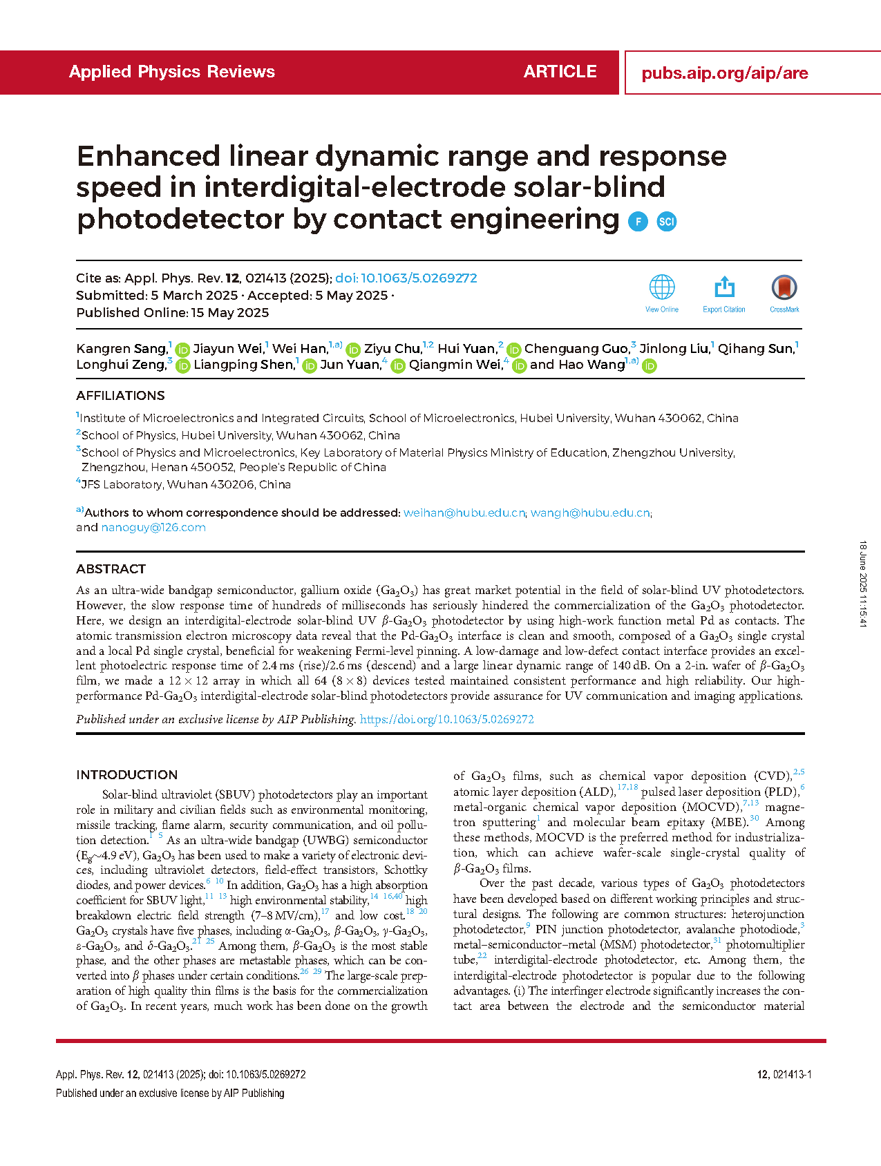
FIG. 1. (a) Schematic diagram of the interdigital-electrode Pd-Ga2O3 photodetector. (b) Band diagram of the Pd-Ga2O3 device. (c) Cross-sectional HAADF image and (d) EDS element mapping images at the Pd-Ga2O3 interface. (e) HAADF image, the magnified image, and the lattice model at the junction area. (f) HAADF image of Ga2O3. (g) HRTEM image and magnified area of the Pd-Ga2O3 interface. (h) SAED patterns of the Ga2O3 and Pd+Ga2O3 mixed area.
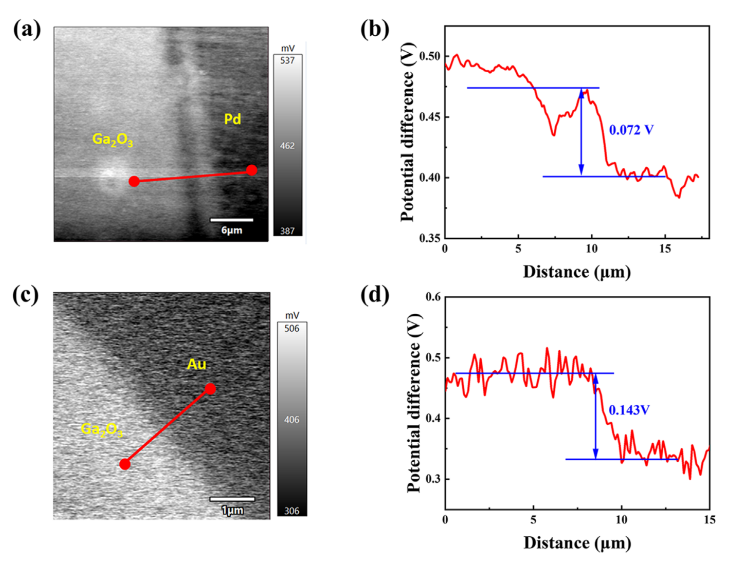
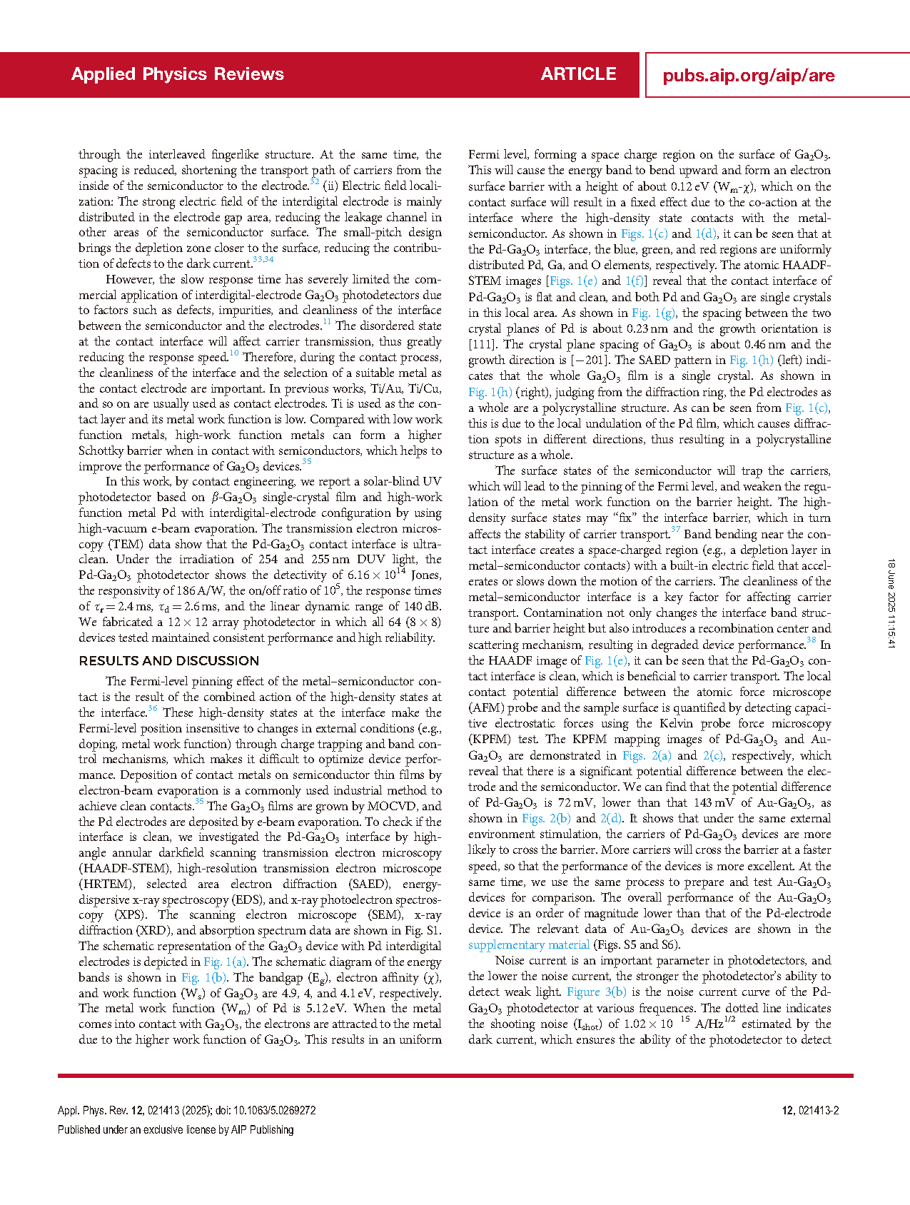
FIG. 2. (a) KPFM mapping image of Pd-Ga2O3 and (b) the corresponding potential difference curve. (c) KPFM mapping image of Au-Ga2O3 and (d) the corresponding potential difference curve.
DOI:
doi.org/10.1063/5.0269272