Member News
【Member News】GAREN SEMI Achieves Wafer-Scale Production of 6-Inch Off-Cut Gallium Oxide Substrates
日期:2025-06-26阅读:939
In February 2025, Hangzhou GAREN SEMI Co., LTD. (hereinafter referred to as "GAREN SEMI") made a new breakthrough in the growth and processing technology of Gallium Oxide crystals, successfully preparing a 6-inch off-cut Gallium Oxide substrate, in which the main surface of the substrate was a (100) plane, off-cut by 4° along the [00-1] direction.
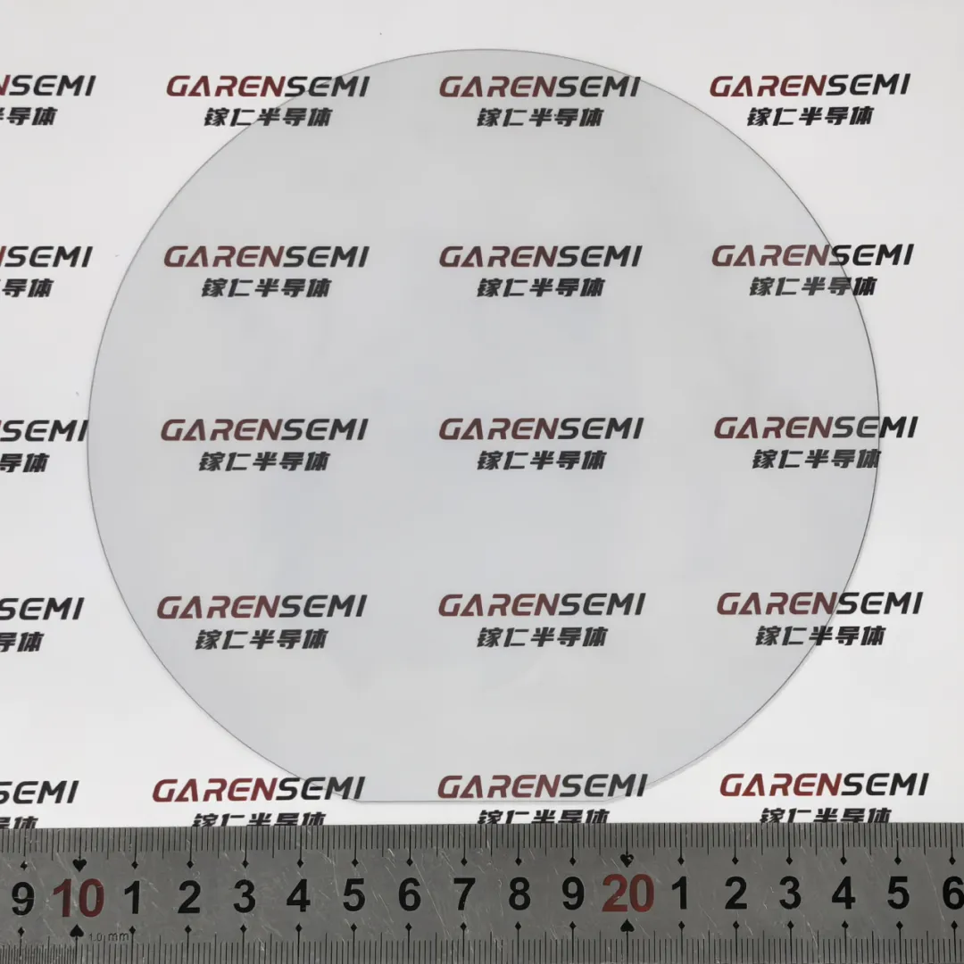
Figure 1 6-inch off-cut Gallium Oxide substrate of GAREN SEMI
Characterization results show that in terms of substrate quality, the XRD full width at half maximum of the substrate is less than 90 arcsec, and the quality has reached the international leading level; In terms of the surface morphology of the substrate, a distinct step surface was formed, which is conducive to step flow epitaxial growth; In terms of wafer flatness parameters, the warp is 14.7 μm, the Bow is 5.7 μm, and the total thickness deviation (TTV) is 5.7 μm. The surface shape parameters have reached the wafer-level standard and are comparable to the level of Silicon Carbide substrate products of the same size.
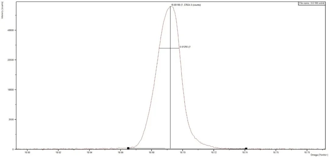
Figure 2 XRD data of 6-inch off-cut Gallium Oxide substrate with GAREN
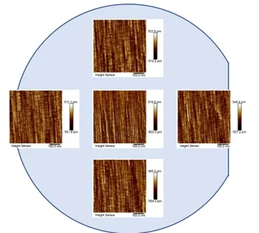
Figure 3 Surface roughness of 6-inch off-cut Gallium Oxide substrate of GAREN
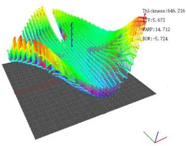
Figure 4 shows the test results of the surface profile parameters of a 6-inch off-cut Gallium Oxide substrate with a GAREN
The Significance of Gallium Oxide Off-Cut Substrates
On (100) tangential Gallium Oxide substrates, epitaxial films tend to grow predominantly in an island growth mode. In the island structure, there are mismatch dislocations to release strain. There are small angular orientation deviations between the islands. After they converge, a boundary layer with high dislocation density will be generated, and at the same time, the surface roughness of the epitaxial layer will increase. Therefore, the island growth pattern should be avoided during epitaxial growth.
The off-cut (100) substrate surface forms a stepped morphology. During epitaxial growth, atoms tend to adsorb and migrate to the step edges, which can transform the growth mode of the epitaxial film into step flow growth, effectively suppresses the formation of lattice defects. Moreover, due to the characteristics of step flow growth, the step flow epitaxial growth surface is almost indistishable from the substrate and still maintains a relatively low roughness.
Furthermore, based on the previous research results of the R&D team, off-cut along the [00-1] direction will expose the (-201) step surface and can also inhibit the formation of twinning defect.
According to a report from the Leibniz Institute in Germany, researchers have successfully fabricated a vertical FinFET device on a (100) Gallium Oxide substrate with a 4° off-cut, achieving an average breakdown field strength of 2.7 MV/cm. (Kornelius Tetzner et al 2023 Jpn.J. Appl. Phys. 62 SF1010). At present, GAREN SEMI has signed a global strategic cooperation agreement with NextGO Epi, an incubated enterprise of the Leibniz Institute for Crystal Growth in Germany. Both sides will collaborate on key research and development based on their technological advantages, focusing on the research and industrialization of ultra-wide band gap semiconductor material Gallium Oxide, and injecting new impetus into the global semiconductor industry.
The Challenges in Off-Cut Gallium Oxide Substrates
Gallium Oxide substrates have significant advantages in chamfer, but to achieve large-scale industrial application, large-sized off-cut substrates need to be fabricated. Compared with small-sized chamfer substrates, the difficulty of preparing large-sized chamfer substrates increases geometrically. The main difficulties are reflected in the following two aspects:
(1) Preparation of Large-Sized Thick Crystal Ingots
Due to the strong anisotropy in the growth of Gallium Oxide single crystal, the main plane of the bulk is usually confined to a few low-index crystal face. However, the (100) plane, characterized by its low surface energy, is the most stable and cost-effective crystal face for the formation of the main plane, thus having a natural advantage in industrialization. However, if off-cut substrates are to be prepared, especially large-sized chamfer substrates, strict requirements are imposed on both the diameter and thickness of the crystal ingot. Take a 6-inch chamfer substrate as an example. To fabricate a 6-inch chamfer substrate, the Gallium Oxide bulk must have a diameter of at least 6 inches and a thickness of more than 11.5mm. Therefore, preparing large-sized thick crystal ingots is the first difficulty faced in fabricating chamfer substrates.
(2) Cleavage Cracking and Surface Profile Variation in Large-Sized Substrates
The Gallium Oxide substrate has two cleavage planes, (100) and (001), which are highly prone to cleavage cracking during the processing. At the same time, the larger the substrate size, the more difficult it is to maintain flatness, and the more difficult it is to control surface profile parameters such as warp, bow, and total thickness variation of the substrate.
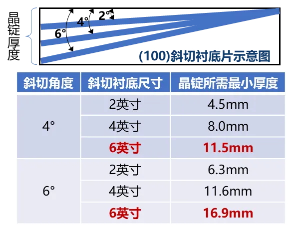
Figure 5 Schematic diagram: Requirements for the thickness of the crystal ingot by off-cut at different angles
In response to the above difficulties, the R&D team of GAREN SEMI carried out systematic research and development efforts.
In terms of crystal growth, the team upgraded the thermal field of the casting method and optimized the process, successfully producing 6-inch-thick ingots with a thickness of over 20mm. In terms of substrate processing, the team, in combination with equipment renovation, comprehensively optimized the processing technology and successfully prepared high-quality 6-inch off-cut substrates, with the substrate surface shape parameters reaching wafer-level standards.
Company Profile
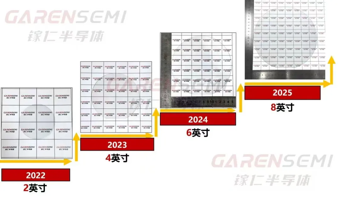
Hangzhou GAREN SEMI Co., Ltd. was established in September 2022. It is a technology-based enterprise specializing in the research and development, production and sales of wide bandgap semiconductor materials and equipment such as Gallium Oxide.
GAREN SEMI leads industry innovation by adopting its independently developed new casting method for single crystal growth technology. It was the world's first to launch an 8-inch Gallium Oxide single crystal substrate, setting an industry record of upgrading one size each year from 2 inches to 8 inches. And have developed the first domestic VB crystal growth equipment dedicated to Gallium Oxide that includes a process package and are now fully available for sale. The research team from Zhejiang University has been deeply involved in the field of Gallium Oxide research, and has achieved key technological breakthroughs in the growth, detection, and quality evaluation of Gallium Oxide single crystals. GAREN SEMI is committed to addressing major national demands. It has mastered core technologies covering the entire chain of Gallium Oxide growth, processing, and epitaxy, and has obtained 14 domestic and international invention patents. It is deeply engaged in continuous innovation in the upstream industrial chain of Gallium Oxide.
The company's products include Gallium Oxide substrates of different sizes, crystal orientations and resistivity, as well as customizable Gallium Oxide seed crystals, etc. The products are mainly used in power electronic devices for the state grid, new energy vehicles, rail transit, 5G communication and other fields. After years of research and development, the company has mastered the core technologies of the entire chain, including equipment development, thermal field design, crystal growth, and crystal processing, and is capable of providing Gallium Oxide substrates with completely independent intellectual property rights. GAREN SEMI is committed to addressing major national demands. It will focus on continuous innovation in the upstream industrial chain of Gallium Oxide and strive to provide product support for the development of China's power electronics and other industries.
For more information about GAREN SEMI and its products
Visit our Web site: http://garen.cc/
Or contact us in the following ways:
Mr. Jiang :15918719807
E-mail :jiangjiwei@garen.cc
Mr. Xia :19011278792
E-mail :xianing@garen.cc