


Paper Sharing
【Domestic Papers】1.4-kV Irradiation-Hardened β-Ga₂O₃ Heterojunction Barrier Schottky Diode Under 10⁷ ions/cm² Fluence and 82.1 MeV⋅cm²/mg LET Environments
日期:2025-06-26阅读:617
Researchers from the Nanjing University have published a dissertation titled "1.4-kV Irradiation-Hardened β-Ga2O3 Heterojunction Barrier Schottky Diode Under 107 ions/cm2 Fluence and 82.1 MeV⋅cm2/mg LET Environments " in IEEE Electron Device Letters.
Project Support
This work was supported in part by the National Key Research and Development Program of China under Grant 2022YFB3605403; in part by Jiangsu Provincial Science and Technology Major Project under Grant BG2024030; in part by Jiangsu Provincial Key Research and Development Program of China under Grant BE2023007-4 and Grant BK20232045; in part by the National Natural Science Foundation of China under Grant 62425403, Grant 62234007, Grant 62293522, Grant 62304102, Grant U21A2071, and Grant U21A20503; and in part by the Open Foundation of Key Laboratory of Laser Devices and Technology of China North Industries Group Company Ltd. under Grant KLLDT202303.
The authors would like to thank the Space Environment Simulation Research Infrastructure (SESRI) and the Frontiers Science Center for Matter Behave in Space Environment of Harbin Institute of Technology for providing the irradiation facilities and technical support.
Background
Ultrawide bandgap neta-gallium oxide (UWBG β-Ga2O3) has garnered significant attention for aerospace electronic systems thanks to its superior material properties, particularly its high threshold displacement energy of lattice atoms. This property makes β-Ga2O3 devices inherently more resistant to radiation-induced displacement damage. To exploit the irradiation tolerance of β-Ga2O3 devices researchers have utilized heavy ions with energies spanning from MeV (germanium, Ge ions) to GeV (tantalum, Ta ions), replicating the harsh conditions of the space environment. However, catastrophic single-event burnout (SEB), characterized by significant derating of breakdown voltage (BV) under irradiation remains a critical 38 challenge. Currently, 1.1-kV β-Ga2O3 power diodes exhibit SEB voltages of only 150∼250 V under irradiation, which is insufficient for high-voltage aerospace applications.
Abstract
Single event burnout (SEB) caused by heavy ion irradiation in space environments poses a significant threat to aerospace power electronic devices. This work demonstrates irradiation-hardened β -Ga2O3 heterojunction barrier Schottky (HJBS) diodes with exceptional SEB capability. The device design incorporates micron-scale deep trenches filled by p-type nickel oxide (NiO) and high-k BaTiO3 field-plate (FP) edge termination. This architecture efficiently extracts radiation-induced positive charges (holes) during single-event irradiation through the trenched-embedded Ni/p-NiO with low Ohmic contact resistance, significantly alleviating charge aggregation while minimizing non-uniform field distributions through strategically engineered charge drainage pathways. As a result, the HJBS device achieves a SEB voltage exceeding 1.4 kV and a SEB degradation rate of only 9.6%. This is the first demonstration of kilovolt-class radiation-hardened diodes, and its performance metrics are the best reported among SiC, GaN, Ga2O3 and Si power diodes to date. This work underscores the great potential of Ga2O3 power diodes for irradiation power applications.
Conclusion
The NiO/β-Ga2O3 HJBS demonstrates robust radiation tolerance through synergistic design: low-resistance Ni/NiO-filled trenches enable efficient hole charge dissipation, while BaTiO3 field plates mitigate edge electric field crowding. This optimized architecture achieves a record-high VSEB of 1436 V and a low SEB degradation rate of 9.6% after 107 heavy-ion strikes at 82.1 MeV·cm2/mg, highlighting the potential of β-Ga2O3 for radiation-hardened power electronics in extreme environments.
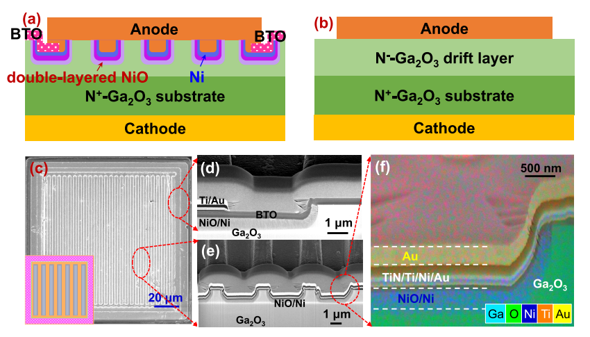
Fig. 1. (a) Schematic of IH- and (b) C-Ga2O3 diodes. (c) Top view scanning electron microscopy (SEM) image of the proposed device, along with the corresponding cross-sectional SEM images of the (d) terminal structure and (e) trenches in the active region. (f) Energy dispersive spectrometer (EDS) elemental mapping images of Ga, Ni, Ti, and Au from a partially enlarged view of (e).
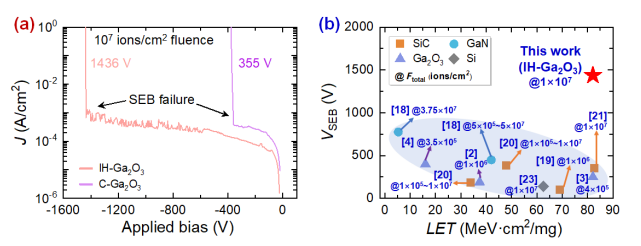
Fig. 2. (a) SEB characteristics of devices under 107 ions/cm2 irradiation condition. (b) Benchmark of VSEB vs. LET under their respective fluence conditions.
DOI:
doi.org/10.1109/LED.2025.3553579
