Paper Sharing
【Domestic Papers】Low Leakage Current β-Ga₂O₃ Self-Aligned Trench Junction Barrier Schottky Diodes
日期:2025-06-26阅读:632
Researchers from the Sun Yat-sen University have published a dissertation titled "Low Leakage Current β-Ga2O3 Self-Aligned Trench Junction Barrier Schottky Diodes" in IEEE Transactions on Electron Devices.
Project Support
This work was supported in part by the National Key Research and Development Program of China under Grant 2024YFE0205300; in part by the Science and Technology Development Plan Project of Jilin Province, China, under Grant YDZJ202303CGZH022; in part by the National Natural Science Foundation of China under Grant 62471504; in part by Shenzhen Institutions of Stability Support Project under Grant 20231127114207001; in part by the High-Level Talent Start-Up Funding Project under Grant RC2024-008; and in part by the Open Fund of the State Key Laboratory of Optoelectronic Materials and Technologies, Sun Yat-sen University, under Grant OEMT-2023-KF-05.
Background
β-gallium oxide (β-Ga2O3), owing to its advantages such as an ultra-wide bandgap and high breakdown field strength, is an ideal material for fabricating high-voltage power diodes. The Junction Barrier Schottky Diode (JBS), an advanced device structure, periodically embeds p-type regions beneath the Schottky contact. This design integrates the low on-voltage characteristic of Schottky diodes with the low reverse leakage current advantage of p-n junction diodes. Under reverse bias, the depletion region formed by the p-n junction expands and merges, thereby shielding the Schottky interface from high electric fields and significantly suppressing leakage current. The Trench Junction Barrier Schottky (TJBS) structure embeds p-type regions into trenches, which provides more effective shielding and enhances device integration density. However, fabricating such a complex TJBS structure—particularly precisely aligning the p-type trenches with the top Schottky contact—typically requires multiple complex lithography and etching processes, which increases manufacturing costs and process complexity.
Abstract
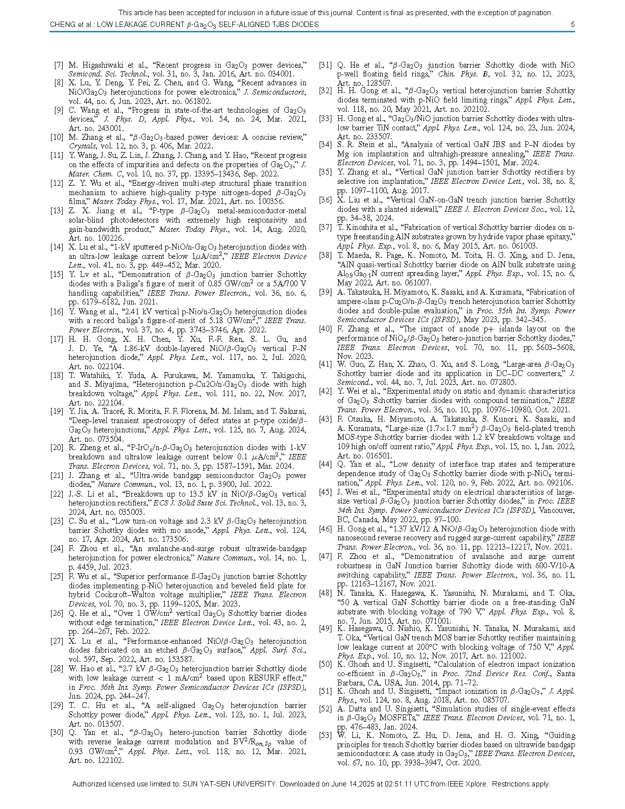
We demonstrate the fabrication of β-Ga2O3 self-aligned trench junction barrier Schottky (TJBS) diodes with a high breakdown voltage (BV) and suppressed reverse leakage current, in which the micrometer-deep trenches were formed using the Schottky anode metal as an etching mask and subsequently covered by a layer of p-type nickel oxide (NiO). High BVs of over 2 kV were achieved in small area devices (0.43 × 0.43 mm2) while maintaining an ultralow reverse leakage current density of around 10−5 A/cm2 until breakdown. A TCAD simulation analysis revealed that the deep trenches covered with p-NiO can effectively reduce the surface electric field of the proposed device and provide sufficient p-shielding effects. Additionally, the packaged large-area β-Ga2O3 TJBS diodes (3 × 3 mm2) show a forward current IF and BV of 15 A/820 V. The results demonstrate that the self-aligned TJBS structure offers critical insights into reducing reverse leakage current and improving high current-handling capabilities in large-area devices.
Conclusion
This study presents the fabrication of β-Ga2O3 self-aligned TJBS diodes, characterized by a high BV and low reverse leakage current. The diodes feature micrometer-deep trenches, formed with Schottky anode metal as an etching mask and subsequently covered with a p-type NiO layer. Small-area diodes (0.43 × 0.43 mm2) achieved BVs over 2 kV with reverse leakage current densities as low as 10−5 A/cm2. TCAD simulations verified that these p-NiO-covered trenches effectively mitigate surface electric fields and offer robust p-type shielding. Additionally, large-area β-Ga2O3 TJBS diodes (3 × 3 mm2) exhibited an IF and BV of 15 A and 820 V. These findings highlight that the self-aligned TJBS structure provides essential insights into reducing reverse leakage current and enhancing the high current-handling capabilities of large-area devices.
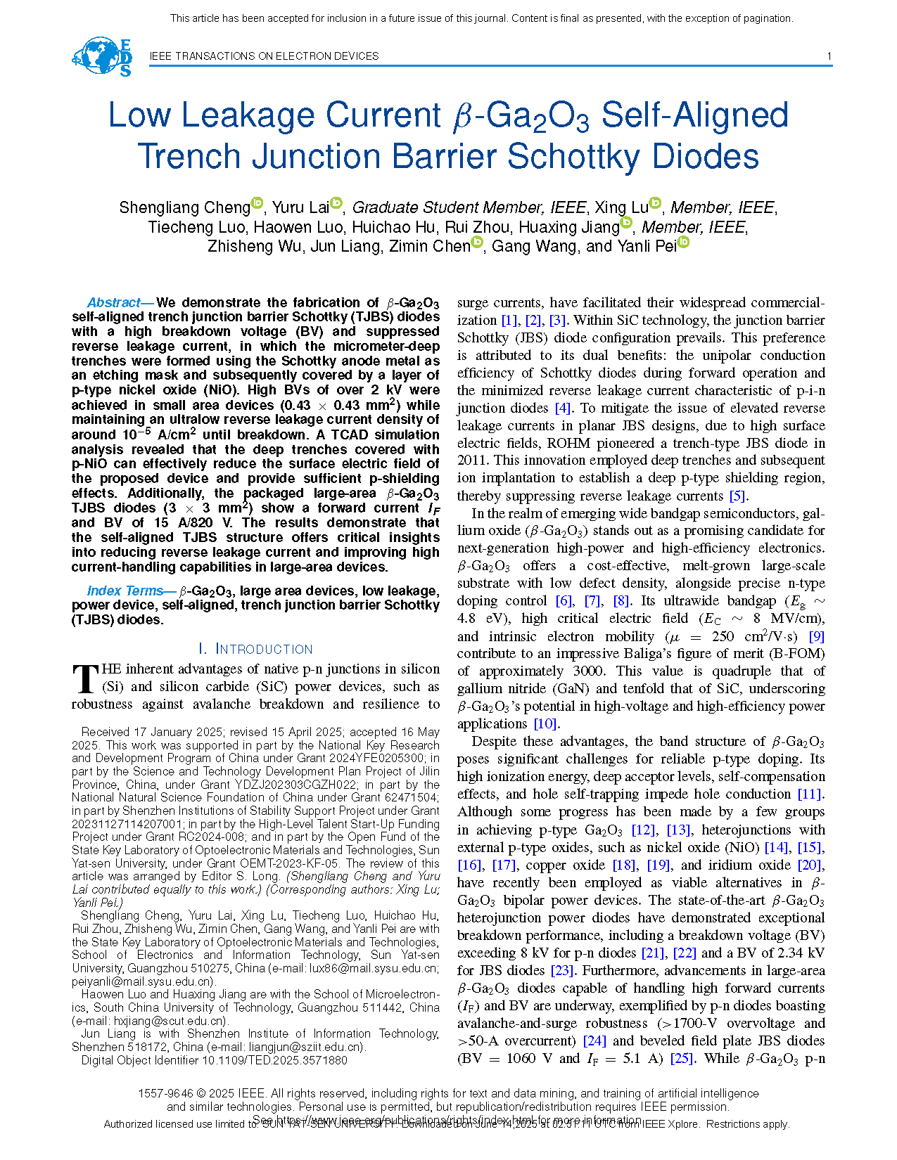
Fig. 1. (a) Cross-sectional schematic illustration of the β-Ga2O3 TJBS fabricated using self-aligned technology, and the key steps involved in its fabrication process. (b) Cross-sectional SEM image showcasing the 1.1-µm deep trench TJBS diode with a fin width of 3 µm. (c) Packaged large-area β-Ga2O3 TJBS diodes. (d) Cross-sectional schematic of the β-Ga2O3 SBD and HJD, both featuring an identical anode diameter of 170 µm. (e) C-V characteristics of the β-Ga2O3 SBD, along with the extracted ND − NA profiles.

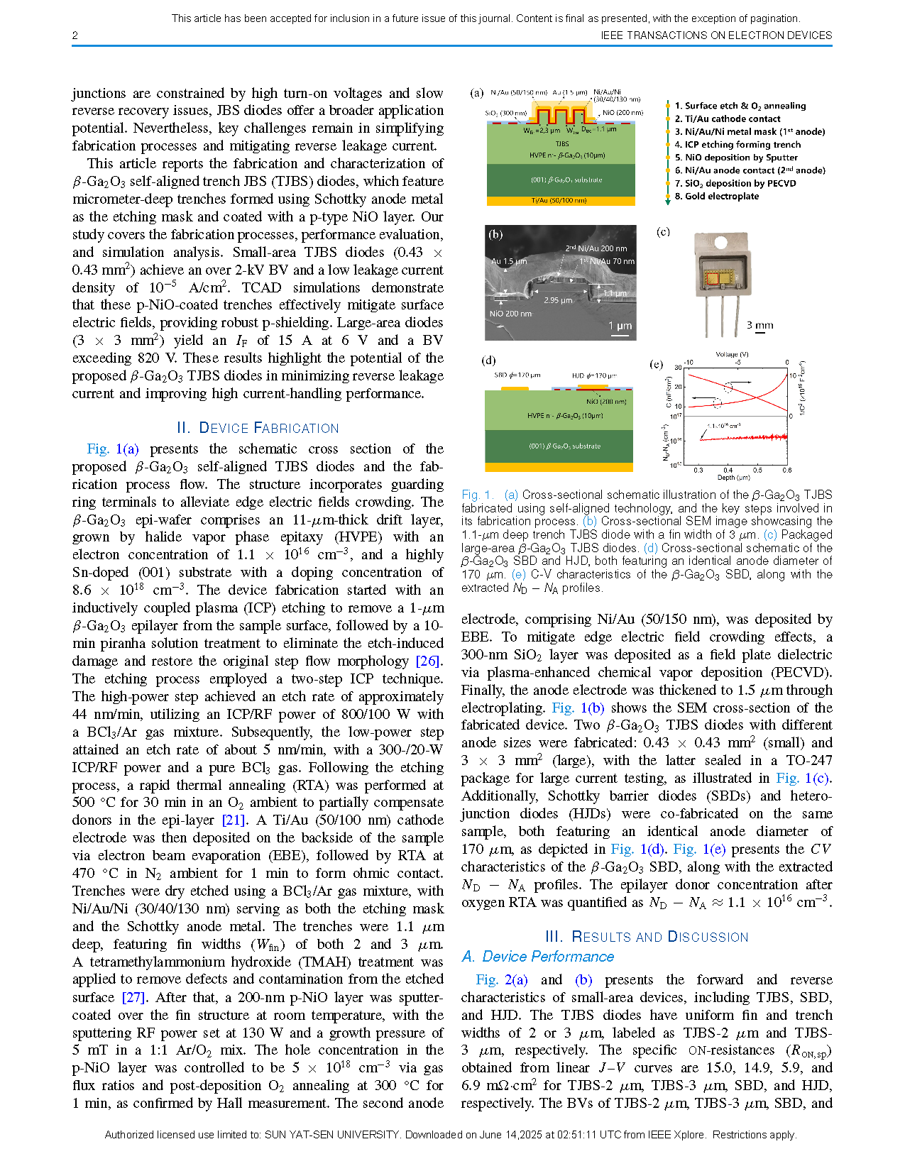
Fig. 2. (a) Forward conduction characteristics and (b) BV characteristics of β-Ga2O3 TJBS diodes featuring a small anode area. (c) Leakage current density at BV versus reported BV and (d) benchmark plot of RON,sp versus BV (defined at a leakage current density of 100 µA/cm2) for reported small-area β-Ga2O3 JBSs, GaN JBSs, and AlN SBDs (<0.5 × 0.5 mm2).
DOI:
doi.org/10.1109/TED.2025.3571880