Paper Sharing
【Domestic Papers】3.9 kV Vertical β-Ga₂O₃ Hetero-Junction Diode With High-Temperature Operational Capability
日期:2025-06-26阅读:607
A research team led by Prof. Kuang Sheng and Prof. Hengyu Wang from the Power Electronic Devices Laboratory (PEDL) of the Collage of Electrical Engineering, Zhejiang University, have published a dissertation titled "3.9 kV Vertical β-Ga2O3 Hetero-Junction Diode With High-Temperature Operational Capability" in ISPSD 2025.
Project support
This work was supported in part by Zhejiang Provincial Natural Science Foundation of China under Grant No. LZ25E070001, and in part by the Delta Power Electronics Science and Education Development Program of Delta Group under Grant No. DREG2023001. The authors thank the ZJU Micro-Nano Fabrication Center, Zhejiang University and Westlake Center for Micro/Nano Fabrication, Westlake University for the facility support and technical assistance in device fabrication.
Background
Power semiconductor devices are the key to achieve high-efficiency energy conversion within power electronic systems. Recently, the rapid development of power semiconductor devices is advanced by wide bandgap (WBG) and ultrawide bandgap (UWBG) semiconductors, along with multidimensional structural innovations. β-Ga2O3 stands out as a promising material for the next generation power electronic devices due to its excellent material properties, such as an ultra-wide bandgap of 4.5-4.9 eV, a decent electron mobility of 250 cm2/V·s, and a high critical electric field of 7-8 MV/cm.
Despite these advantages, the inherent difficulty in achieving native p-type doping in Ga2O3 imposes significant limitations on device performance. This challenge prevents the device from reaching its material limitations, In contrast, p-type nickel oxide (NiO) is an attractive material for Ga2O3 power devices due to its wide bandgap and tunable p-type doping capabilities. The NiO can not only serve as hetero-junction to conduct current, but also manage electric field by providing the negative charges for charge compensation during blocking state.
Abstract
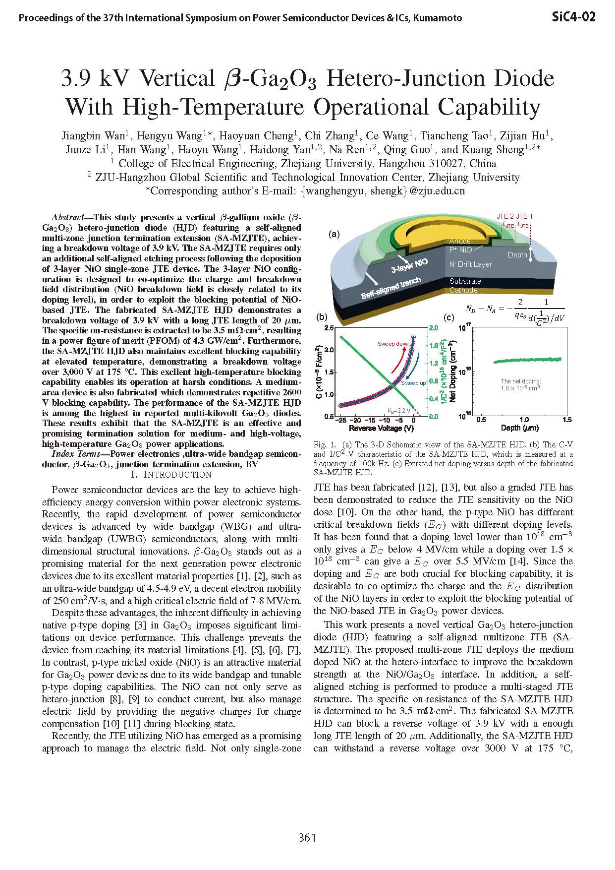
This study presents a vertical β-gallium oxide (β-Ga2O3) hetero-junction diode (HJD) featuring a self-aligned multi-zone junction termination extension (SA-MZJTE), achieving a breakdown voltage of 3.9 kV. The SA-MZJTE requires only an additional self-aligned etching process following the deposition of 3-layer NiO single-zone JTE device. The 3-layer NiO configuration is designed to co-optimize the charge and breakdown field distribution (NiO breakdown field is closely related to its doping level), in order to exploit the blocking potential of NiO-based JTE. The fabricated SA-MZJTE HJD demonstrates a breakdown voltage of 3.9 kV with a long JTE length of 20 μm. The specific on-resistance is extracted to be 3.5 mΩ·cm2, resulting in a power figure of merit (PFOM) of 4.3 GW/cm2. Furthermore, the SA-MZJTE HJD also maintains excellent blocking capability at elevated temperature, demonstrating a breakdown voltage over 3,000 V at 175 °C. This excllent high-temperature blocking capability enables its operation at harsh conditions. A medium-area device is also fabricated which demonstrates repetitive 2600 V blocking capability. The performance of the SA-MZJTE HJD is among the highest in reported multi-kilovolt Ga2O3 diodes. These results exhibit that the SA-MZJTE is an effective and promising termination solution for medium- and high-voltage, high-temperature Ga2O3 power applications.
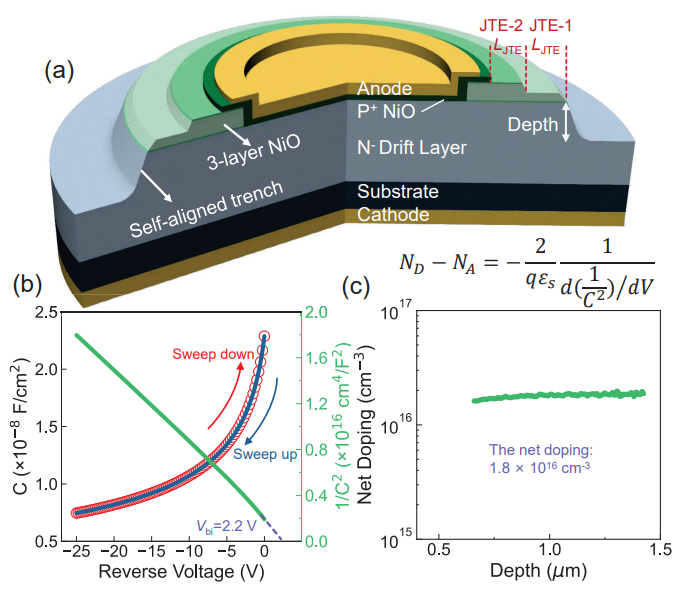
Fig. 1. (a) The 3-D Schematic view of the SA-MZJTE HJD. (b) The C-V and 1/C2-V characteristic of the SA-MZJTE HJD, which is measured at a frequency of 100k Hz. (c) Extrated net doping versus depth of the fabricated SA-MZJTE HJD.
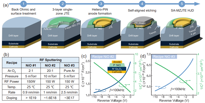
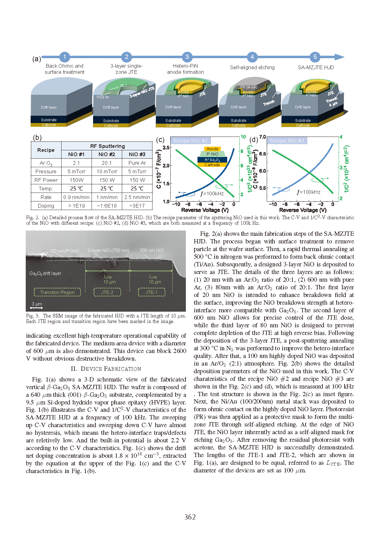
Fig. 2. (a) Detailed process flow of the SA-MZJTE HJD. (b) The recipe parameter of the sputtering NiO used in this work. The C-V and 1/C2-V characteristic of the NiO with different recipe: (c) NiO #2, (d) NiO #3, which are both measured at a frequency of 100k Hz.