Paper Sharing
【Domestic Papers】Fabrication of porous Ga₂O₃/GaN heterojunction for ultraviolet photodetector application
日期:2025-06-24阅读:578
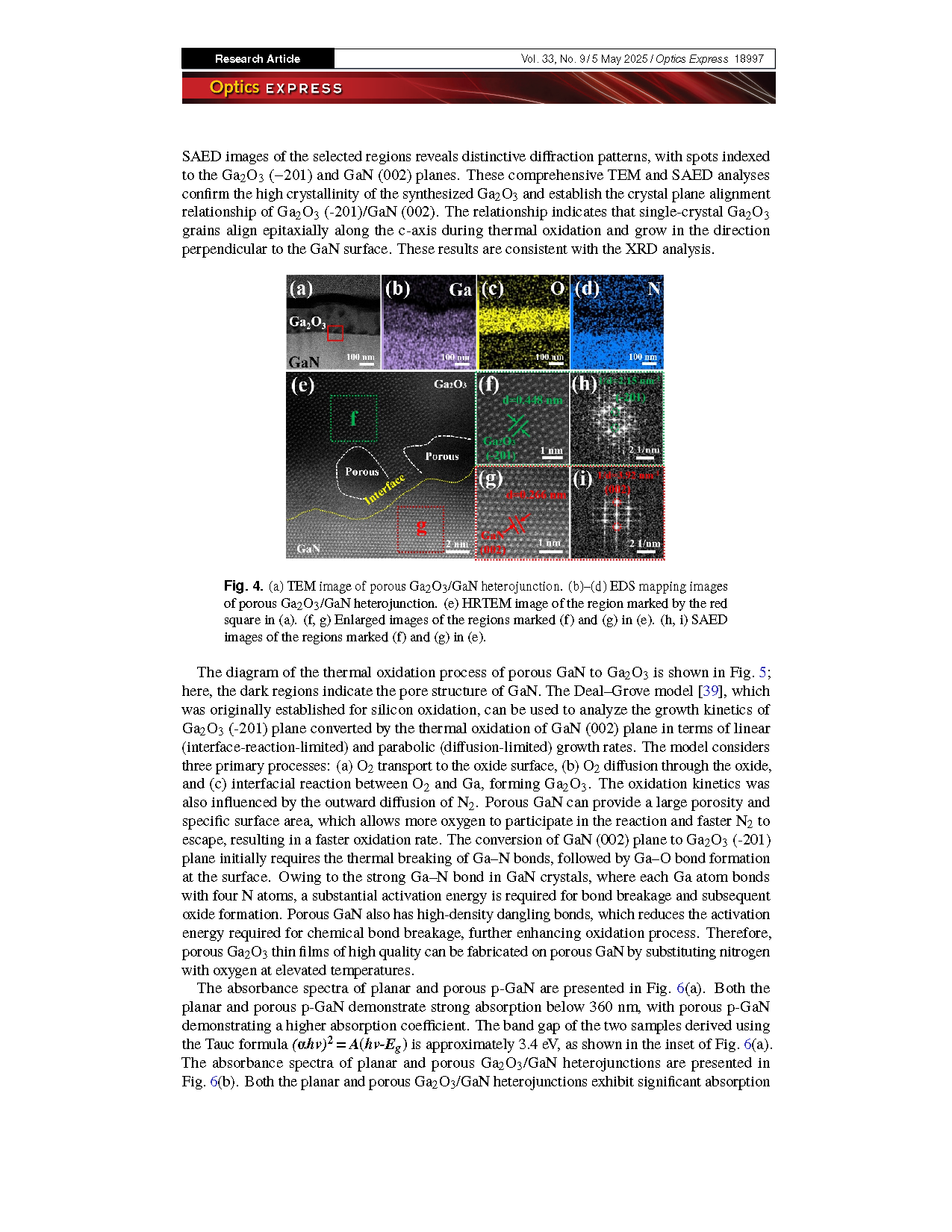
Researchers from the Taiyuan University of Technology have published a dissertation titled "Fabrication of porous Ga2O3/GaN heterojunction for ultraviolet photodetector application" in Optics Express.
Project Support
Shanxi Provincial Key Research and Development Project (202302150101001); Shanxi-Zheda Institute of Advanced Materials and Chemical Engineering (2021SX-AT002, 2022SX-TD018); National Natural Science Foundation of China (21972103, 61904120).
Background
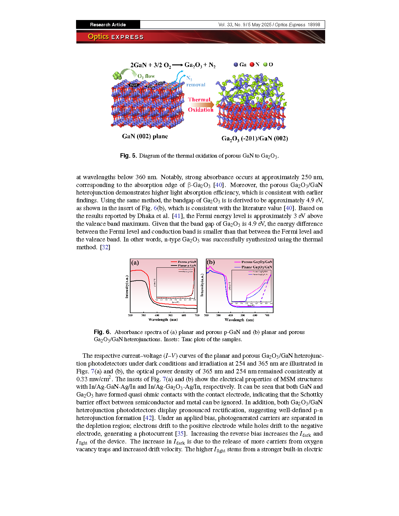
UV photodetectors are widely used in both military and civilian applications such as astronomical imaging systems, chemical/biological analysis, bioaerosol detection, ozone hole monitoring, and secure communications. Among the photodetectors reported to date, p-n junction-type UV photodetectors have attracted considerable research interest owing to their many advantages, which include a low dark current (Idark), low power consumption, and high responsivity (R). As a significant fourth-generation semiconductor material, Ga2O3 is a promising candidate for UV-detection applications because of its wide band gap (4.4–5.2 eV), high UV transmittance (over 80%), large edge absorption coefficient (up to 105 cm−1), and excellent chemical and thermal stability. Ga2O3 is generally considered an n-type semiconductor owing to its inherent oxygen deficiency. However, due to the self compensation effect of oxygen vacancies and the deep energy level of acceptors, the p-type Ga2O3 is difficult to obtain , which greatly limits the development of Ga2O3-based p-n junction-type photodetectors. In response to this challenge, researchers have proposed the integration of Ga2O3 with p-type semiconductors such as NiO, SnO2 , and GaN, to construct heterojunction photodetectors. In particular, GaN has received increased attention because of its high carrier mobility, wide direct band gap (3.4 eV), and good chemical and thermal stability; moreover, when combined with Ga2O3, it shows minimal lattice mismatch and a low conduction band shift.
Abstract
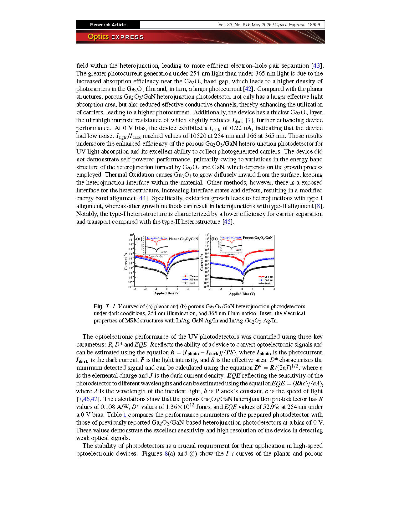
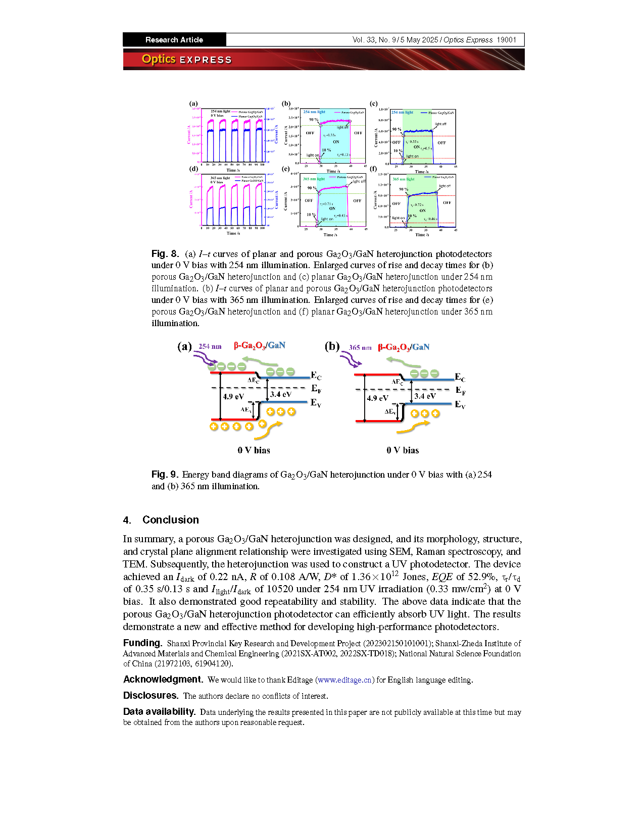
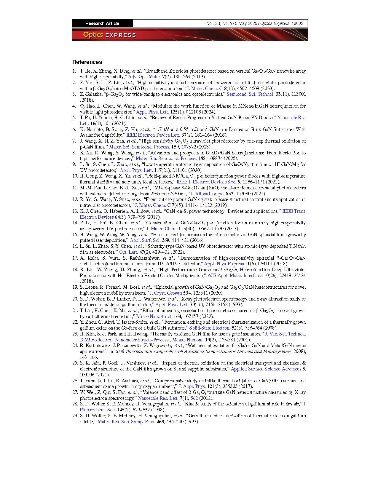
Ga2O3/GaN heterojunction has important applications in optoelectronic devices. Understanding optoelectronic performance and interface relationships of the heterojunction is the key to designing optimal devices. Herein, a porous Ga2O3/GaN heterojunction is systematically investigated. Porous GaN is initially fabricated via ultraviolet-assisted electrochemical etching and porous Ga2O3 is subsequently converted from porous GaN by thermal oxidation. Compared with planar Ga2O3/GaN heterojunction, porous Ga2O3/GaN heterojunction has higher crystal quality. Porous Ga2O3/GaN heterojunction exhibits a light/dark current ratio of 10520, a responsivity of 0.108 A/W, an external quantum efficiency of 52.9%, a detectivity of 1.36 × 10¹² Jones, and the response time of 0.35 s/0.13 s under 254 nm UV irradiation (0.33 mw/cm2) at 0 V bias. Additionally, the operating mechanism of the device is further explored through energy band structure and carrier-transport process diagrams. This study provides valuable insights and paves the way for developing next-generation optoelectronic devices based on Ga2O3/GaN heterojunction.
Conclusion
In summary, a porous Ga2O3/GaN heterojunction was designed, and its morphology, structure, and crystal plane alignment relationship were investigated using SEM, Raman spectroscopy, and TEM. Subsequently, the heterojunction was used to construct a UV photodetector. The device achieved an Idark of 0.22 nA, R of 0.108 A/W, D* of 1.36 × 10¹² Jones, EQE of 52.9%, τr /τd of 0.35 s/0.13 s and Ilight/Idark of 10520 under 254 nm UV irradiation (0.33 mw/cm2 ) at 0 V bias. It also demonstrated good repeatability and stability. The above data indicate that the porous Ga2O3/GaN heterojunction photodetector can efficiently absorb UV light. The results demonstrate a new and effective method for developing high-performance photodetectors.
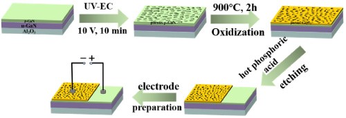
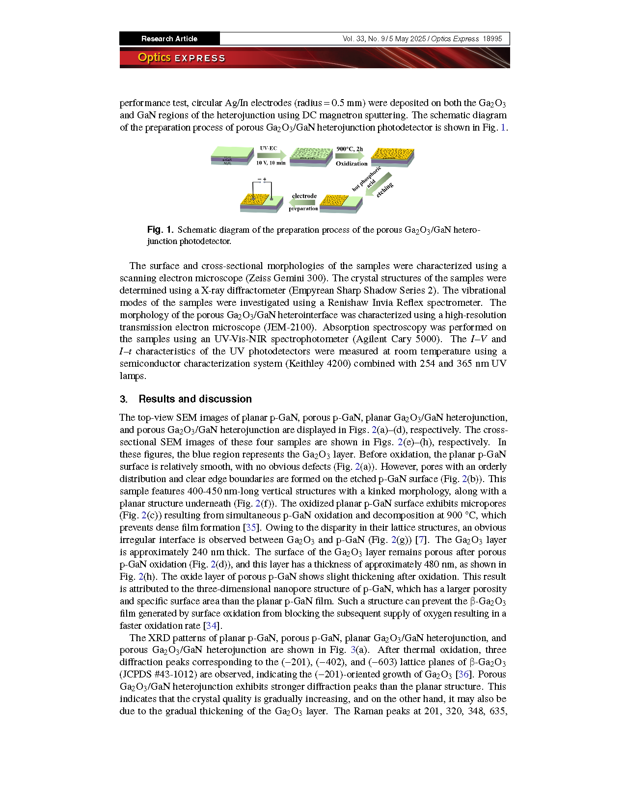
Fig. 1. Schematic diagram of the preparation process of the porous Ga2O3/GaN heterojunction photodetector.
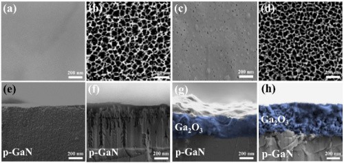
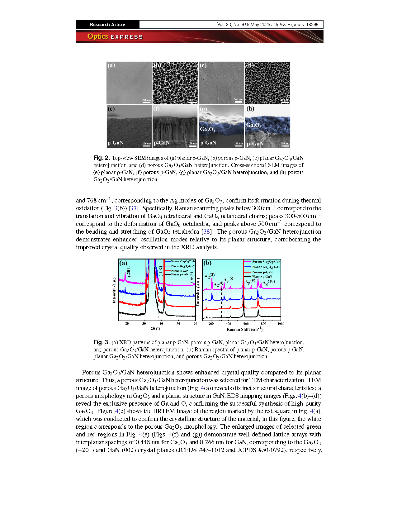
Fig. 2. Top-view SEM images of (a) planar p-GaN, (b) porous p-GaN, (c) planar Ga2O3/GaN heterojunction, and (d) porous Ga2O3/GaN heterojunction. Cross-sectional SEM images of (e) planar p-GaN, (f) porous p-GaN, (g) planar Ga2O3/GaN heterojunction, and (h) porous Ga2O3/GaN heterojunction.
DOI:
doi.org/10.1364/OE.561140