Paper Sharing
【International Papers】Growth and properties of Sn-doped sol-gel Ga₂O₃ thin films
日期:2025-06-23阅读:572
Researchers from the University of Canterbury have published a dissertation titled "Growth and properties of Sn-doped sol-gel Ga2O3 thin films" in Journal of Vacuum Science & Technology A.
Corresponding Author

Martin Allen is a Professor in electrical engineering at the University of Canterbury. He has a BSc (Hons) degree in Physics from the University of Bristol, UK, an MSc in Plasma Physics from the University of Oxford, UK, and a PhD in Electrical Engineering from the University of Canterbury.
His current research interests include the fundamental properties and commercial device applications of metal oxide semiconductors, particularly those that are optically active in the UV spectrum.
Background
Wide bandgap transparent semiconducting oxides (TSOs) are an interesting class of electronic material combining high optical transparency with strong electrical conductivity—properties that are usually mutually exclusive in nature. Ga2O3 is one such TSO with an ultrawide bandgap (Eg ∼ 4.8 eV) that extends its transparency into the ultraviolet-A and ultraviolet-B regions. It also has a very high thermal stability (m.p. ∼1900 °C) and one of the highest-known semiconductor breakdown strengths (∼8 MV cm−1). Consequently, Ga2O3 has attracted significant interest for a wide range of applications, including high-efficiency power electronics, high-operating temperature electronic devices, and deep-ultraviolet solar-blind photodetectors. Ga2O3 has six different crystal phases, α, β, γ, η, ɛ, and κ, with the monoclinic β phase being the most thermodynamically stable and also the most studied, with some research also conducted on amorphous Ga2O3.
Ga2O3 thin films are usually produced using vapor deposition techniques such as pulsed laser deposition (PLD), molecular beam epitaxy (MBE), and chemical vapor deposition. These techniques involve the use of equipment that is expensive to operate and in the case of Ga2O3 suffer from low growth rates due to the formation of volatile suboxides.
Abstract
Ga2O3 is an ultrawide bandgap semiconductor with a very high thermal stability and breakdown strength that is attracting significant interest for use in high-efficiency power electronics and solar-blind UV photodetectors. However, Ga2O3 films are usually expensive to produce by physical vapor deposition due to the creation of volatile suboxides that can significantly limit the achievable growth rates. In this work, a low cost, solution-based sol-gel technique was used to rapidly produce Ga2O3 films. High quality (100% transparent, 0.3 nm root-mean-squared roughness) Sn-doped Ga2O3 films of up to 500 nm thickness were grown by sol-gel on c-plane sapphire substrates. The resulting films were amorphous and exhibited sufficient electrical conductivity for the fabrication of PtOx/Pt Schottky diodes with four orders of magnitude rectification (at ±10 V). Post-growth annealing of the films in N2 at temperatures higher than 600 °C introduced polycrystalline β-Ga2O3 phases but did not produce any improvement in electrical conductivity. This work demonstrates the ability of the highly scalable sol-gel technique to rapidly produce low-cost Sn-doped Ga2O3 films and the first Schottky diode devices fabricated on intentionally doped sol-gel Ga2O3 thin films.
Conclusion
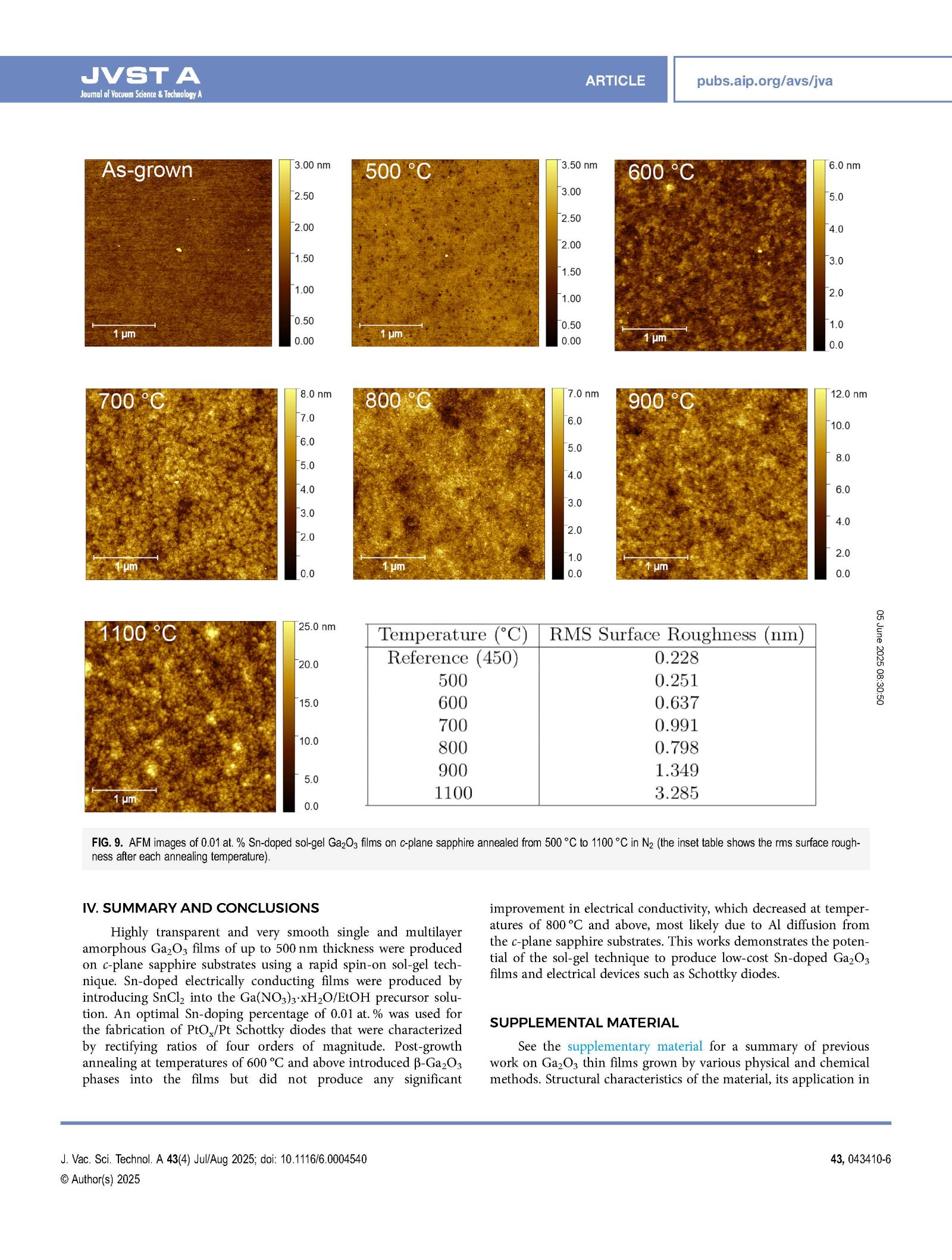
Highly transparent and very smooth single and multilayer amorphous Ga2O3 films of up to 500 nm thickness were produced on c-plane sapphire substrates using a rapid spin-on sol-gel technique. Sn-doped electrically conducting films were produced by introducing SnCl2 into the Ga(NO3)3⋅xH2O/EtOH precursor solution. An optimal Sn-doping percentage of 0.01 at. % was used for the fabrication of PtOx/Pt Schottky diodes that were characterized by rectifying ratios of four orders of magnitude. Post-growth annealing at temperatures of 600 °C and above introduced β-Ga2O3 phases into the films but did not produce any significant improvement in electrical conductivity, which decreased at temperatures of 800 °C and above, most likely due to Al diffusion from the c-plane sapphire substrates. This works demonstrates the potential of the sol-gel technique to produce low-cost Sn-doped Ga2O3 films and electrical devices such as Schottky diodes.
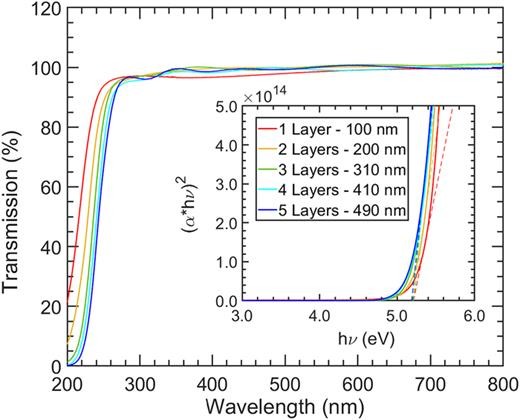
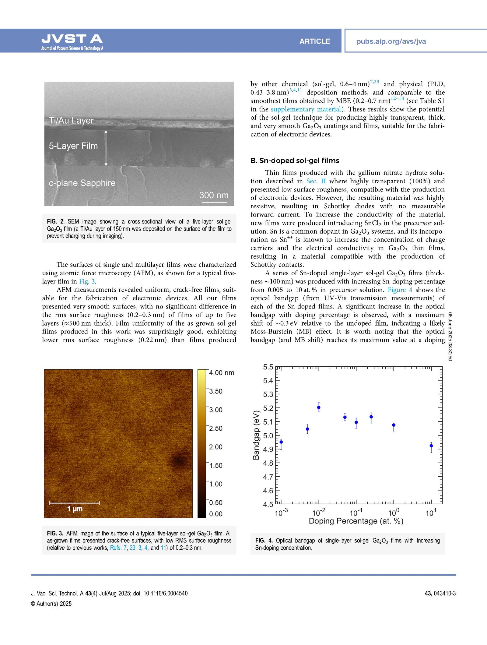
FIG. 1. Transmission spectra of 0.01 at. % Sn-doped sol-gel Ga2O3 films of increasing thickness. Inset: Tauc plots used to determine the bandgap of the material, constructed from the corresponding transmission spectra in Fig. 1.
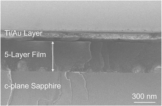
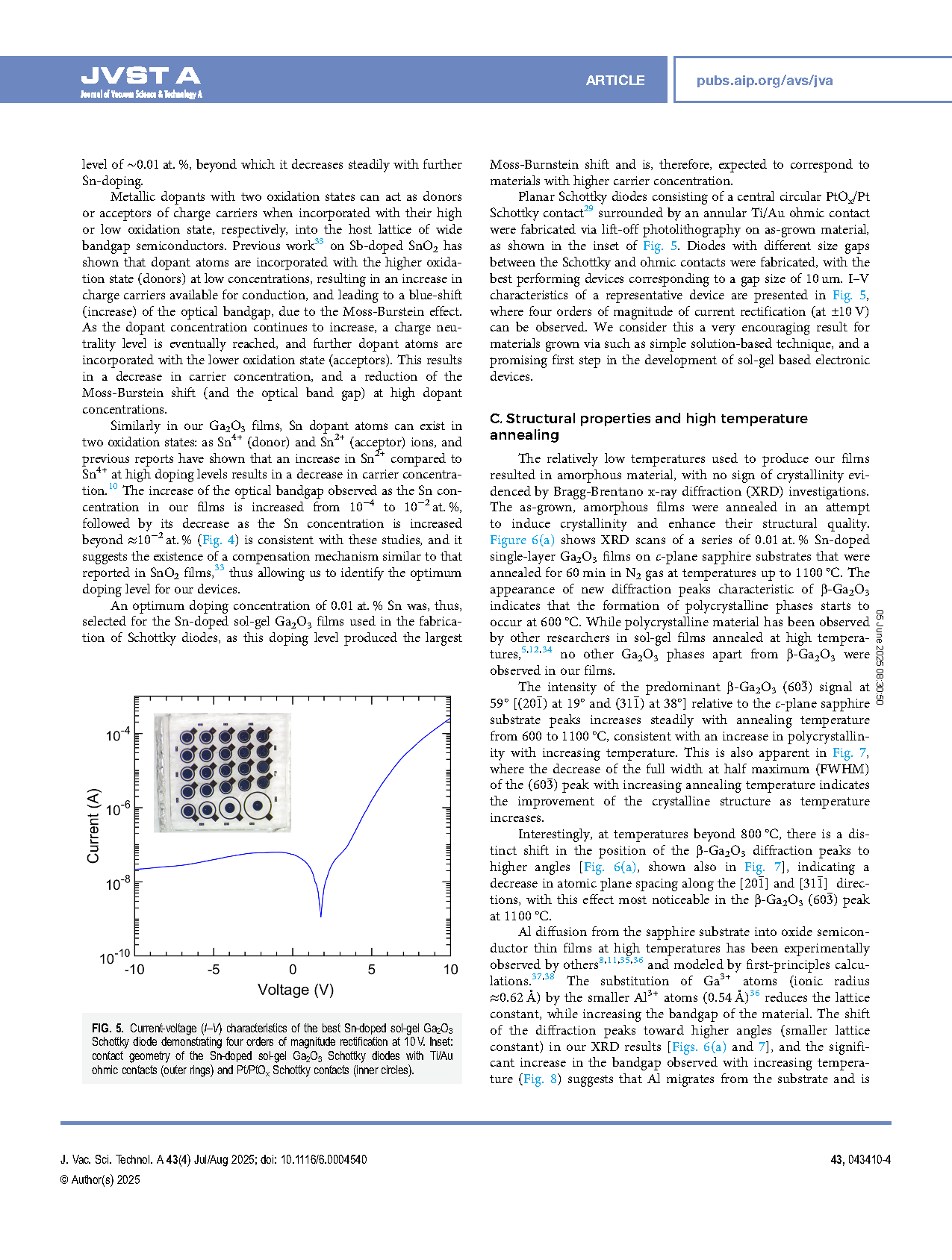
FIG. 2. SEM image showing a cross-sectional view of a five-layer sol-gel Ga2O3 film (a Ti/Au layer of 150 nm was deposited on the surface of the film to prevent charging during imaging).
DOI:
doi.org/10.1116/6.0004540