


Discover
【Knowledge Discover】Understanding Thin-Film Fabrication: A Look at MOCVD, Magnetron Sputtering and PECVD Techniques
日期:2025-06-23阅读:2342
This article will introduce several methods for preparing thin films. In semiconductor processing techniques, photolithography and etching are the most frequently mentioned, followed by epitaxy (thin film) processes.
Why is thin-film technology needed for chip manufacturing?
For example, many people like to eat pancakes. If a pancake is not seasoned, it won't taste good or have a bad texture when baked. Some people, who prefer a salty taste, brush a layer of broad bean paste on the surface of the pancake, and those who prefer a sweet taste brush a layer of maltose on the surface.
After brushing the sauce, the layer of salty or sweet sauce on the surface of the pancake can be called a film, and its appearance changes the whole flavor of the pancake, and the pancake itself is called the substrate.
Of course, in the process of chip processing, there are many functions of films, and there are also many methods for preparing films. This article briefly introduces several common methods for preparing films, including MOCVD, magnetron sputtering, PECVD, etc...
1. Metal-Organic Chemical Vapor Deposition (MOCVD)
The MOCVD epitaxial growth system is a highly complex and precise device that plays a crucial role in the preparation of high-quality semiconductor films and nanostructures.
The MOCVD system consists of five core components, each of which performs different but interrelated functions, jointly ensuring the efficiency and safety of the material growth process.
(1) Gas delivery system: The main responsibility of this subsystem is to precisely control the delivery of various reactants to the reaction chamber, including the metering of reactants, the time and sequence of delivery, and the regulation of the total gas flow rate.
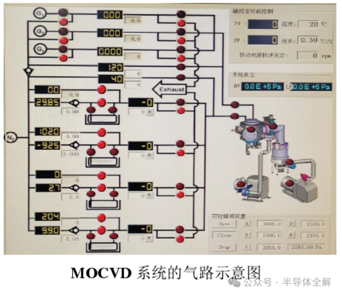
It consists of several subsystems, including the carrier gas supply subsystem for carrying reactants, the supply subsystem for providing metal-organic (MO) sources, the supply subsystem for supplying hydrides, and the growth/venting multi-way combination valve for controlling the gas flow direction, as shown in the diagram below, which is a schematic diagram of the MOCVD growth system gas path.
(2) Reaction chamber system: It is the core of the MOCVD system and is responsible for the actual material growth process.
This section includes a graphite base for carrying the substrate, a heater for heating the substrate, a temperature sensor for monitoring the temperature of the growth environment, an optical inspection window, and an automatic loading and unloading manipulator for automating the loading and unloading of the substrate to improve production efficiency. The picture below shows the heating status of the MOCVD reaction chamber.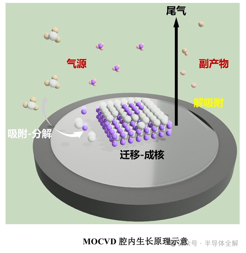
(3) Growth control system: Composed of a programmable controller and control computer, it is responsible for the precise control and monitoring of the entire MOCVD growth process.
The controller handles the acquisition, processing and output of various signals, while the control computer is responsible for recording and monitoring each stage of material growth to ensure the stability and repeatability of the process.
(4) In-situ monitoring system: including reflectance correction infrared radiation pyrometer, reflectance monitoring and warpage monitoring equipment.
This system can monitor key parameters during the material growth process in real time, such as film thickness and homogeneity, as well as the temperature of the substrate, thereby achieving immediate adjustment and optimization of the growth process.
(5) Tail gas treatment system: It is responsible for handling toxic particles and gases produced during the reaction process.
By means of cracking or chemical catalysis, these harmful substances are effectively decomposed and absorbed to ensure a safe and environmentally compliant operating environment.
In addition, MOCVD equipment is usually installed in ultra-clean rooms equipped with advanced safety alarm systems, effective ventilation devices and strict temperature and humidity control systems. These auxiliary facilities and safety measures not only ensure the safety of the operators, but also improve the stability of the growth process and the quality of the final product.
The design and operation of MOCVD systems reflect the high standards of precision, repeatability and safety in the field of semiconductor material preparation and are one of the key technologies for manufacturing high-performance electronic and optoelectronic devices.
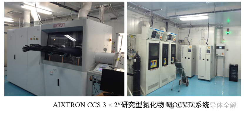
The Closed-Coupled Showerhead (CCS)MOCVD system in the equipment chamber is used for growing epitaxial thin films.
The design of this system adopts a unique spray head structure. Its core feature lies in effectively reducing pre-reactions and achieving effective gas mixing. These gases are respectively injected into the reaction chamber through the alternately distributed spray holes on the spray head, where they are fully mixed, thereby enhancing the uniformity and efficiency of the reaction.
The design of the spray head structure allows the reaction gas to be evenly distributed over the substrate located beneath it, ensuring consistent concentration of the reaction gas at all locations on the substrate. This is crucial for forming an epitaxial film with uniform thickness.
In addition, the rotation of the graphite disk further promotes the homogenization of the chemical reaction boundary layer, resulting in more uniform growth of the epitaxial film. This rotation mechanism helps to reduce local concentration differences by thinning the boundary layer of the chemical reaction, thereby enhancing the overall uniformity of film growth.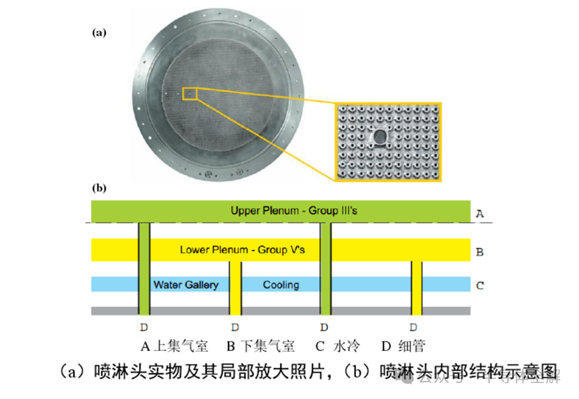
2.Magnetron Sputtering
Magnetron sputtering is a physical vapor phase deposition technique commonly used for thin film deposition and surface coating.
It uses a magnetic field to release atoms or molecules of a target material from the surface of the target and to form a thin film on the surface of the substrate material.
This technique is widely used in the manufacturing of semiconductor devices, optical coatings, ceramic coatings and many other fields.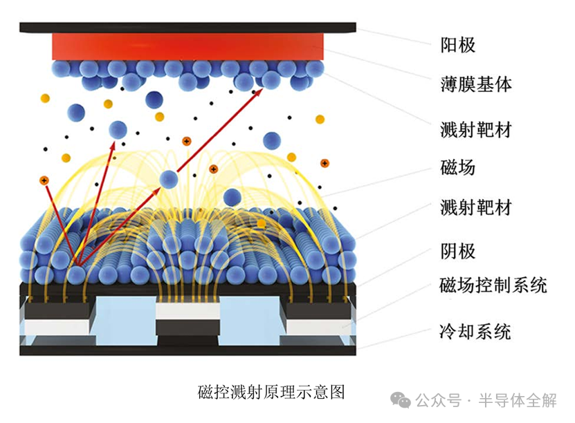
The principle of magnetron sputtering is as follows:
Target material selection: The target material is the target material to be deposited on the substrate material. It can be metal, alloy, oxide, nitride, etc. Target material is usually attached to a device called a sputtering gun.
Vacuum environment: The sputtering process must be carried out in a high vacuum environment to prevent the interaction between gas molecules and the target material. This helps ensure the purity and uniformity of the deposited film.
3 Ionizing gas: An inert gas (such as argon) is usually introduced during the sputtering process to ionize it into a plasma. These ions, under the influence of a magnetic field, form an electron cloud known as an "electron cloud plasma."
Magnetic field application: Apply a magnetic field between the target material and the substrate material. This magnetic field binds the electron cloud plasma to the surface of the target material, thereby maintaining a high energy state.
Sputtering process: By applying high-energy electron cloud plasma, atoms or molecules of the target material are hit and released. These released atoms or molecules are deposited on the surface of the substrate material in the form of vapor, forming a thin film.
The advantages of magnetron sputtering include:
Uniformity of deposited films: The magnetic field helps control the transport of ions, resulting in uniform film deposition, which keeps the thickness and properties of the films consistent across the entire substrate surface.
Preparation of complex alloys and compounds: Magnetron sputtering can be used to prepare complex alloy and compound films that may be more difficult to achieve with other deposition techniques.
Controllability and modulation: By adjusting sputtering parameters such as the composition of the target material, gas pressure, and deposition rate, the properties of the film, such as thickness, composition, and microstructure, can be precisely controlled.
High quality films: Magnetron sputtering can typically produce high quality, dense and uniform films with good adhesion and mechanical properties.
Versatility: It is suitable for a variety of material types, including metals, oxides, nitrides, etc., and thus has a wide range of applications in different fields.
Low-temperature deposition: Compared with other techniques, magnetron sputtering can be carried out at low temperatures or even room temperature, making it suitable for applications that are sensitive to the temperature of the substrate material.
Overall, magnetron sputtering is a highly controllable and flexible thin film preparation technique suitable for a wide range of applications, from electronic devices to optical coatings, etc.
3. Plasma Enhanced Chemical Vapor Deposition
Plasma Enhanced Chemical Vapor Deposition (PECVD) technology is widely used in the preparation of various thin films (such as Silicon, Silicon Nitride and Silicon Dioxide, etc.).
A schematic diagram of the PECVD system is shown below.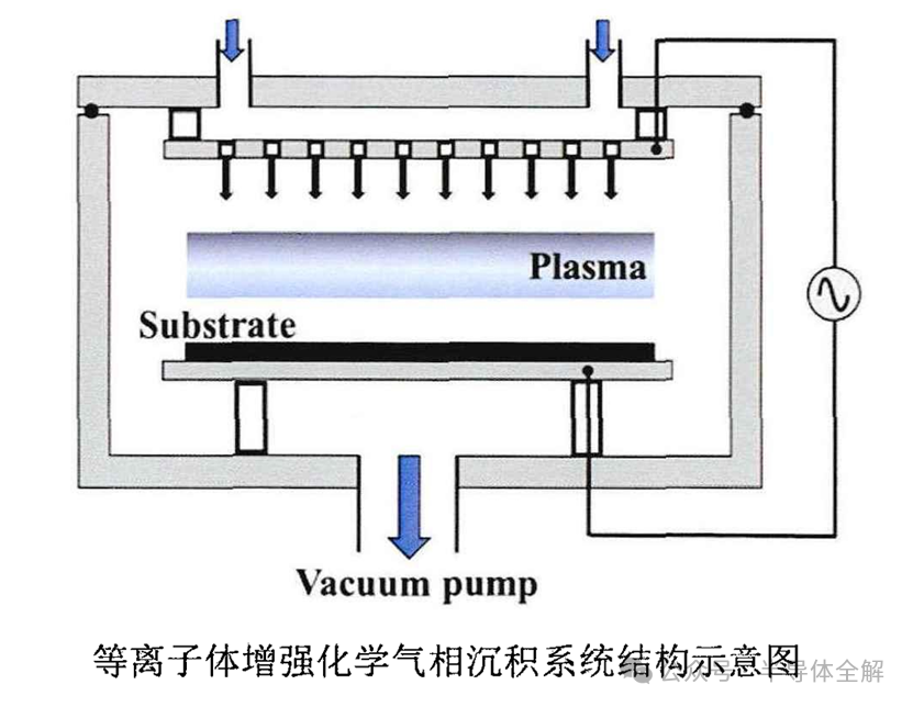
The basic principle of the PECVD system is to fill the deposition chamber with gaseous substances containing thin-film components, and use glow discharge to cause chemical reactions in the gaseous substances to generate plasma, which then deposits on the substrate to grow the thin-film material.
The main methods to excite glow discharge are radio frequency excitation, direct current high voltage excitation, pulse excitation and microwave excitation.
The films prepared by PECVD have good uniformity in both thickness and composition. In addition, the films deposited by this method have strong adhesion and can achieve high deposition rates at lower deposition temperatures.
Generally speaking, the growth of thin films mainly includes the following three processes:
The first step is that the reactive gas, under the excitation of an electromagnetic field, glow discharges to produce plasma.
In this process, electrons collide with the reactive gas, causing a primary reaction that leads to the decomposition of the reactive gas to produce ions and active groups.
In the second step, the various products produced by the primary reaction move towards the substrate, while the various active groups and ions undergo secondary reactions to form secondary products.
In the third step, various primary and secondary products reaching the substrate surface are adsorbed and react with the surface, accompanied by the re-release of gaseous phase molecules.
4.Thin-Film Characterization Techniques
(1) X-Ray Diffraction (XRD)
XRD(X-ray diffraction) is a technique commonly used to analyze the structure of crystals.
It reveals information such as lattice parameters, crystal structure, and crystal orientation of a material by measuring the diffraction patterns of X-rays by the crystal structure within the material.
XRD is widely used in fields such as materials science, solid-state physics, chemistry, and geology.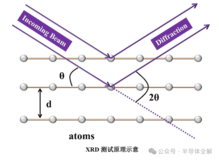
Working principle: The basic principle of XRD is based on Bragg's law, which states that when an incident beam of light hits a crystal sample, X-ray diffraction occurs when the array of atoms or ions in the lattice is in a specific arrangement. The Angle and intensity of the diffraction can provide information about the structure of the crystal.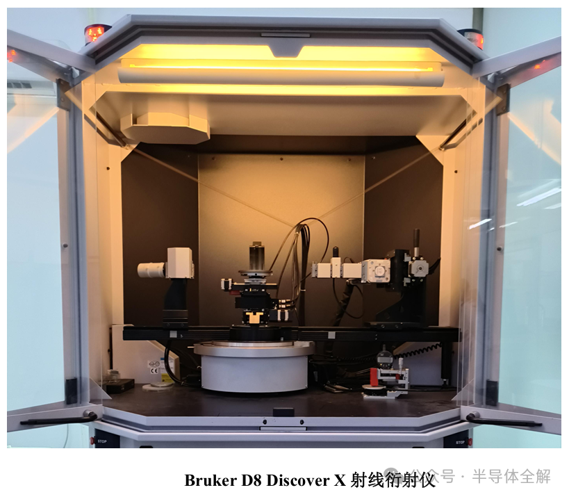
Instrument composition: A typical XRD instrument consists of the following parts:
X-ray source: A device that emits X-rays, typically using a tungsten or copper target to produce X-rays.
Sample stage: A platform for placing samples, which can be rotated to adjust the Angle of the samples.
X-ray detector: Used to measure the intensity and Angle of the diffracted light.
Control and analysis system: A software system including the control of the X-ray source, data acquisition, analysis, and interpretation.
Application fields: XRD has important applications in many fields, including but not limited to:
Crystallographic studies: used to resolve the crystal structure of a crystal, determine lattice parameters and crystal orientation.
Material characterization: Analyze information such as the crystal structure, phase composition, and crystal defect of the material.
Chemical analysis: Identify the crystal structure of inorganic and organic compounds and study the interactions between molecules.
Thin film analysis: For studying the crystal structure, thickness and lattice matching of thin films, etc.
Mineralogy and geology: Used to identify the type and content of minerals and to study the composition of geological samples.
Drug development: Analyzing the crystal structure of drugs helps to understand their properties and interactions.
Overall, XRD is a powerful analytical technique that can help scientists and engineers gain a deep understanding of the crystal structure and properties of materials, thereby promoting research and application in materials science and related fields.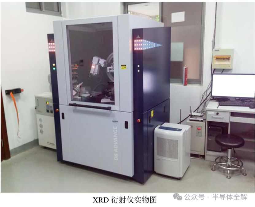
(2) Scanning Electron Microscopy (SEM)
Scanning Electron Microscope (SEM) is a kind of common microscope, by using electron beam rather than a beam of light to illuminate its sample, so as to realize high resolution and surface morphology observation.
The SEM is widely used in materials science, biology, geology and other fields.
Here is the basic working principle of SEM:
SEM uses an electron gun to generate an electron beam. This electron gun is similar to the electron gun in a Cathode-Ray Tube (CRT), generating high-energy electrons. The electron beam passes through a collimation system, including a series of electron lenses, to focus and collimate the electron beam, ensuring its stability and focus. Under the control of the scanning coil, the electron beam scans the surface of the sample.
The position of the electron beam can be precisely controlled to generate scanned pixels on the sample.
The sample is placed on the sample stage of the SEM. The sample needs to be conductive because in SEM, the electron beam needs to interact with the sample surface to generate secondary electrons, etc. When a high-energy electron beam strikes the surface of a sample, it interacts with the atoms and molecules within the sample. These interactions can lead to the scattering, escape and excitation of electrons, generating a variety of signals. SEM detects multiple signals generated from the sample surface, mainly including secondary electrons (SE) and backscattered electrons (BSE).
These signals provide information about the topography, structure, and composition of the sample surface. By controlling the scanning position of the electron beam on the sample, the SEM can obtain pixel information of the sample surface. This information is processed and displayed by a computer to produce images of the sample surface with high resolution.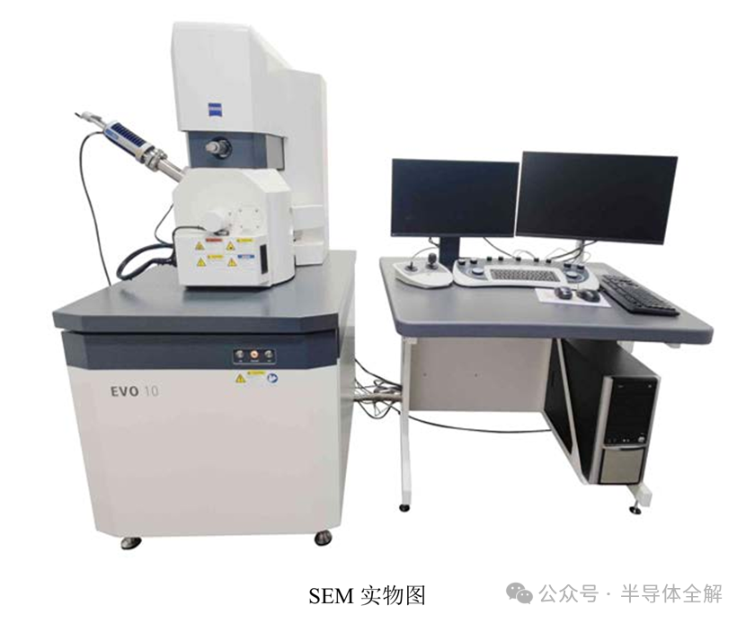
(3) Atomic Force Microscopy (AFM)
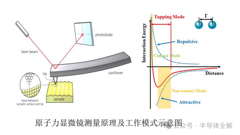
Atomic force microscopy (AFM) is a high-resolution microscopy technique that is primarily used to observe atomic-scale and nanoscale features on sample surfaces. Its working principle is based on the interaction between the probe and the sample surface, and it acquires the topography and topological information of the sample surface by measuring the positional changes of the probe.
In AFM, a very small probe is used, typically a nanoscale tip made of silicon or other material. The probe is attached to the scanning head via a cantilever or piezoelectric device, with the tip of the probe close to the surface of the sample. When the probe approaches the surface of the sample, interactions occur between the atoms and molecules of the sample and the probe, including electrostatic forces, Van Der Waals forces and chemical bond interactions, etc. Control the movement of the cantilever or piezoelectric device to maintain a certain force between the tip of the probe and the surface of the sample.
AFM uses a feedback system to maintain a constant force between the probe and the sample. When the height or position of the probe changes, the feedback system automatically adjusts the position of the cantilever to maintain a constant force. The probe and the sample move relatively, usually on a two-dimensional grid, forming a scan. At each scan point, the unevenness of the sample surface causes a change in the position of the probe tip. Topological information about the sample surface can be obtained by measuring the positional changes of the probe. Ultimately, the collected data is processed to produce a high-resolution topological image of the sample surface.
AFM has a wide range of applications in several fields. It is used in fields such as materials science, biology, and nanotechnology to help researchers gain a deep understanding of the surface topography and structure of materials, and even manipulate nanoscale structures.
The advantages of AFM include high resolution, non-destructiveness and multiple working modes, making it a powerful tool for nanoscale observation and research.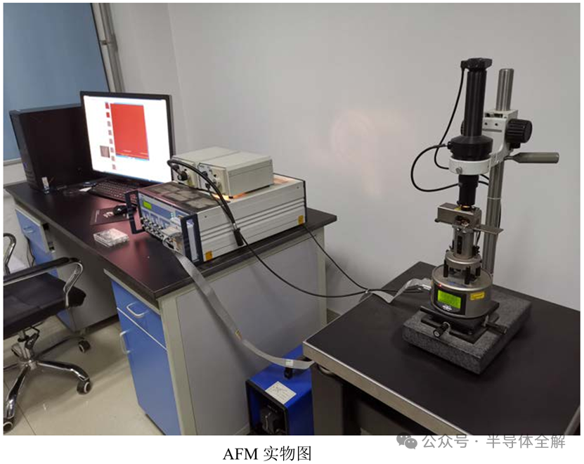
References:
(1) Yu Miao's Research on Gallium Oxide Heterojunction Photodetector [D].
(2) Wang Bingxiang’s Research on GAN-based high gain ultraviolet detector [D].
(3) Zheng Xiantong’s Molecular beam epitaxy InGaN alloy and its photoconductive behavior [D].
(4) Li Qingyun's Research on Silicon and Lithium Niobate Composite Films and Related Photonic Devices [D].
