Paper Sharing
【Member Papers】Xi’an Jiaotong University---Mechanism of Improving Al₂O₃/β-Ga₂O₃ Interface After Supercritical Fluid Process at a Low Temperature
日期:2025-06-18阅读:624
Researchers from the Xi’an Jiaotong University have published a dissertation titled "Mechanism of Improving Al2O3/β-Ga2O3 Interface After Supercritical Fluid Process at a Low Temperature" in IEEE Transactions on Electron Devices.
Project support
This work was supported in part by the National Natural Science Foundation of China under Grant 62204198 and in part by the Joint Funds of the National Natural Science Foundation of China under Grant U23A20367.
Background
The wide bandgap semiconductor devices have become more attractive in power electronics systems. The performances of wide bandgap semiconductor devices, such as the stabilities, reliabilities, and applications, are heavily influenced by the properties of interface states between semiconductor and dielectric layers. As an ultrawide bandgap semiconductor (4.9 eV), gallium oxide (β-Ga2O3) has recently attracted much more attention. Exceptional performances of the β-Ga2O3 devices, including high breakdown voltage and fast switching characteristics, have been reported in specific technologies. However, unlike the GaN high electron mobility transistor (HEMT) and metal–oxide–semiconductor HEMT (MOSHEMT) with buried channels, β-Ga2O3 can only form a depletion-mode metal–oxide–semiconductor field-effect transistor (MOSFET). Therefore, a high-quality dielectric/β-Ga2O3 interface plays an essential role in forming high-performance MOSFETs. In general, high-k dielectric, high conduction band offset, and high dielectric/β-Ga2O3 interface quality are significant concerns in obtaining high-performance devices.
Abstract
β-Ga2O3, a wide bandgap semiconductor, has gained attention for its high breakdown voltage and fast switching properties. However, challenges exist because of high interface densities at the Al2O3/β-Ga2O3 interface, which greatly impacts the performance and reliability of metal-oxide–semiconductor field-effect transistor (MOSFET) devices. As a low-temperature solution, the supercritical fluid process (SCFP) is introduced to the fabrication process of Al2O3/β-Ga2O3 metal-oxide–semiconductor capacitor (MOSCAP), which effectively reduces the oxygen vacancies and interface defects, in particular avoiding the damage to the materials caused by high temperature. The near-interface traps are decreased by two times, and the interface states are reduced by five times. As a result, the breakdown electric field is improved from 6.01 to 8.47 MV cm−1. The mechanism of the SCFP is explored and explained by using different measurement and analysis methods. Deep-level transient spectroscopy (DLTS) results indicate that the defect concentration of SCFP devices decreases and the electron capture interface increases. Supercritical fluid treatment can passivate the traps by reducing O vacancies in the Al2O3. The study concludes that the proposed SCFP significantly improves the dielectric/semiconductor interface, which can greatly enhance the performance of transistors.
Conclusion
In conclusion, the Al2O3/β-Ga2O3 MOSCAPs were fabricated. The SCFP treatment was first developed to improve the interface quality of the Al2O3/β-Ga2O3 interface. The near-interface traps Nbt decreased from 5.6 × 10¹¹ to 3.6 × 1011 cm−2, and the interface states Dit at 0.2 eV below EC reduced from 1.29 × 10¹² to 2.54 × 10¹¹ eV−1 cm−2 for the SCF samples. The DLTS results indicate that the trap energy-level position of SCF devices is deeper, the defect concentration decreases, and with a deeper trap emission energy, which further supports the improvement of the interface quality of the devices. In addition, the breakdown electric field was improved from 6.01 to 8.47 MV cm−1 after the SCFP treatment. Moreover, XPS analysis revealed that the SCFP treatment can passivate the traps by reducing O vacancies in the Al2O3. This work demonstrated the novel SCFP treatment’s effectiveness in improving the interface quality of the β-Ga2O3 MOS structure at low temperatures. It is the first to systematically study the SCFP action and effect on Al2O3/β-Ga2O3 MOS devices, which provides a detailed method description, testing characterization, and mechanism analysis. Other oxide interfaces used in β-Ga2O3 are also very worthwhile to study. SCFP’s high efficiency, low-cost process consumption, and simple process flow make it promising for application in the manufacturing process. This work provides a systematic research methodology and lays a solid foundation for the subsequent related works.
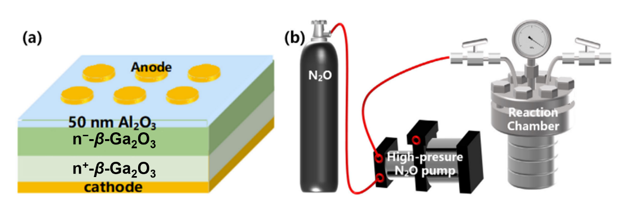
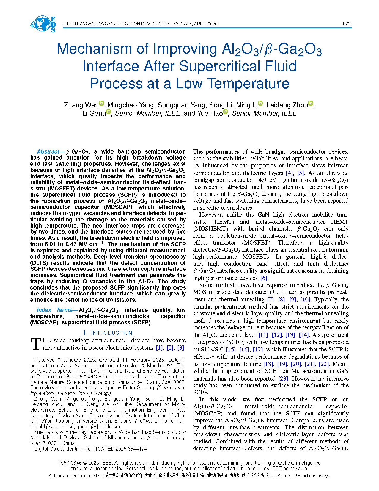
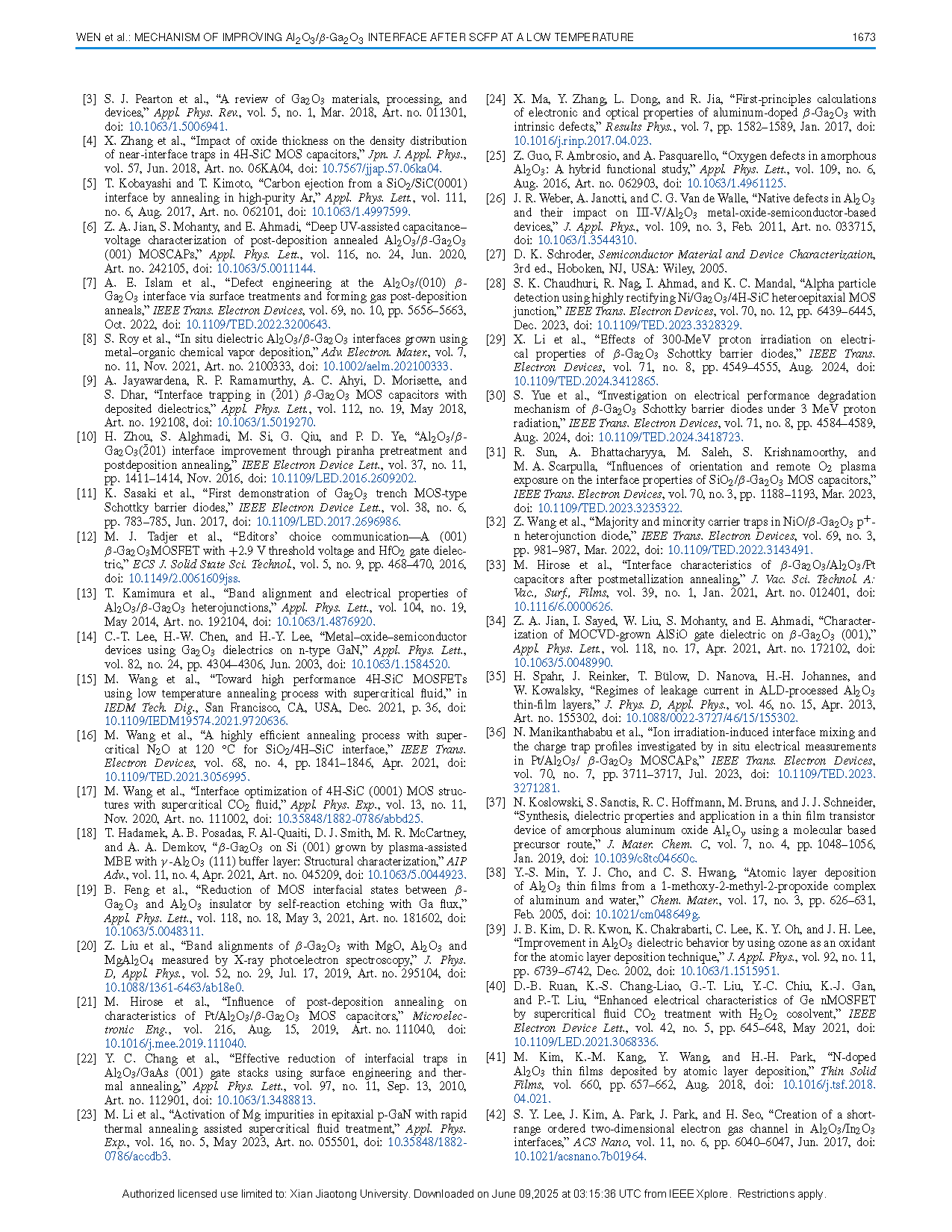
Fig. 1. (a) Cross-sectional schematic of Al2O3/β-Ga2O3 (001) MOSCAP. (b) Diagram of SCFP equipment.
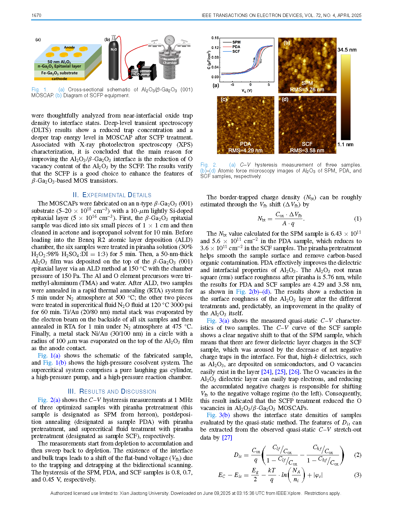
Fig. 2. (a) C–V hysteresis measurement of three samples. (b)–(d) Atomic force microscopy images of Al2O3 of SPM, PDA, and SCF samples, respectively.
DOI:
doi.org/10.1109/TED.2025.3544174