Paper Sharing
【Member Papers】Xidian University --- β-Ga₂O₃ Photodetectors with High-Performance Enhanced by Field Control via p-Type NiO Interlayer
日期:2025-06-16阅读:832
Researchers from the Xidian University have published a dissertation titled "β-Ga2O3 Photodetectors with High-Performance Enhanced by Field Control via p-Type NiO Interlayer" in Journal of Alloys and Compounds.
Acknowledgments
This work was supported by the National Key R&D Program of China (No. 2022YFB3605402), the National Natural Science Foundation of China (under Grants 62274132, 62004151, 62274126), the China Scholarship Council program (Project ID: 202406960106), the Natural Science Basic Research Program of Shaanxi under Grants 2024JC-YBMS474, 2024JC-YBQN-0647, Wuhu Science and Technology Project (applied basic research) under Grant 2022jc01.
Background
Gallium oxide (Ga2O3), one of the new generation wide bandgap semiconductors, has a high breakdown field strength and will help in the fabrication of power devices with great performance. Furthermore, the bandgap of Ga2O3 is approximately 4.9 eV, which signifies that the light absorption of Ga2O3 film terminates in the solar-blind region. Due to the presence of the ozone layer, sunlight within the wavelength range of approximately 200–280 nm is absorbed. Photodetectors operating within this wavelength range would have significant applications. Ga2O3, with its natural advantage, suggests that it will achieve an excellent response without the need for an optical filter for its application. The structure of the Ga2O3 film photodetector includes the Metal-Semiconductor-Metal (MSM), heterogeneous p-n junction, Schottky Barrier Diode (SBD), and Metal-Oxide-Semiconductor (MOS). Among them, MSM photodetectors with a simple structure often obtain a high photo-dark current ratio (PDCR).
Abstract
Gallium oxide (Ga2O3) film exhibiting the solar-blind absorption cutoff characteristic holds considerable potential for application in UV photodetectors. The material defects in the device will introduce the recombination region for the photodetector, especially at the interface of the Ga₂O₃ heterojunction. The photogenerated carriers, generated within the Ga2O3 film, will inevitably be influenced by these high recombination centers during their transportation. Avoiding or minimizing this region can improve the performance of the photodetector. The p-n junction, with its depletion region, generates an electric field that drives the carriers away from the recombination region. However, due to the Ga2O3 p-type doping difficulty, our work focuses on the growth of single-crystal NiO/β-Ga₂O₃ films by Mist-CVD and the fabrication of field-controlled photodetectors. The hole concentration in the NiO film is adjusted by doping with different concentrations of Li⁺. Compared with a photodetector without the NiO interlayer, the performance of the photodetector with the structure of NiO (1 % Li⁺-doped)/β-Ga₂O₃ exhibits a significant improvement, which achieved the maximum responsivity of 1002.5 A/W, and a high peak detectivity of 3.31 × 10¹⁵ Jones.
Highlights
·Single-crystal NiO and β-Ga2O3 are epitaxial grown by low-cost Mist-CVD.
·The p-type NiO layer provides an electric field that helps photogenerated carriers move away from the recombination region.
·The solar blind photodetector with the structure achieves a maximum R of 1002.5 A/W and a high peak D* of 3.31 × 10¹⁵ Jones.
Summary
In conclusion, our work has prepared a single-crystal heterojunction film with the structure of Sapphire/NiO/β-Ga2O3 using Mist-CVD. By doping different concentrations of LiOH into the NiO precursor, NiO films with varying hole concentrations were successfully fabricated. Benefiting from the electric field controlled by the depletion region, the photodetector with the structure of NiO(1 % Li+-doped)/β-Ga2O3 achieves a maximum R of 1002.5 A/W, and a high peak D* of 3.31 × 10¹⁵ Jones. Our work aims to provide a low-cost material epitaxial growth method and contribute to the advancement of Ga2O3-based devices.
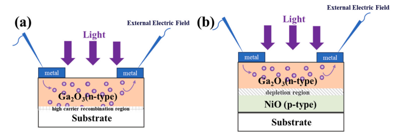
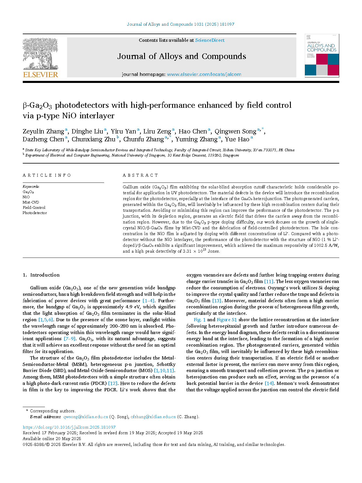
Fig. 1. (a) The schematic diagrams of an n-type Ga2O3 device without a p-type layer. (b)The schematic diagrams of an n-type Ga2O3 device with a p-type layer.
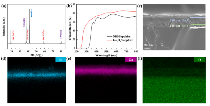
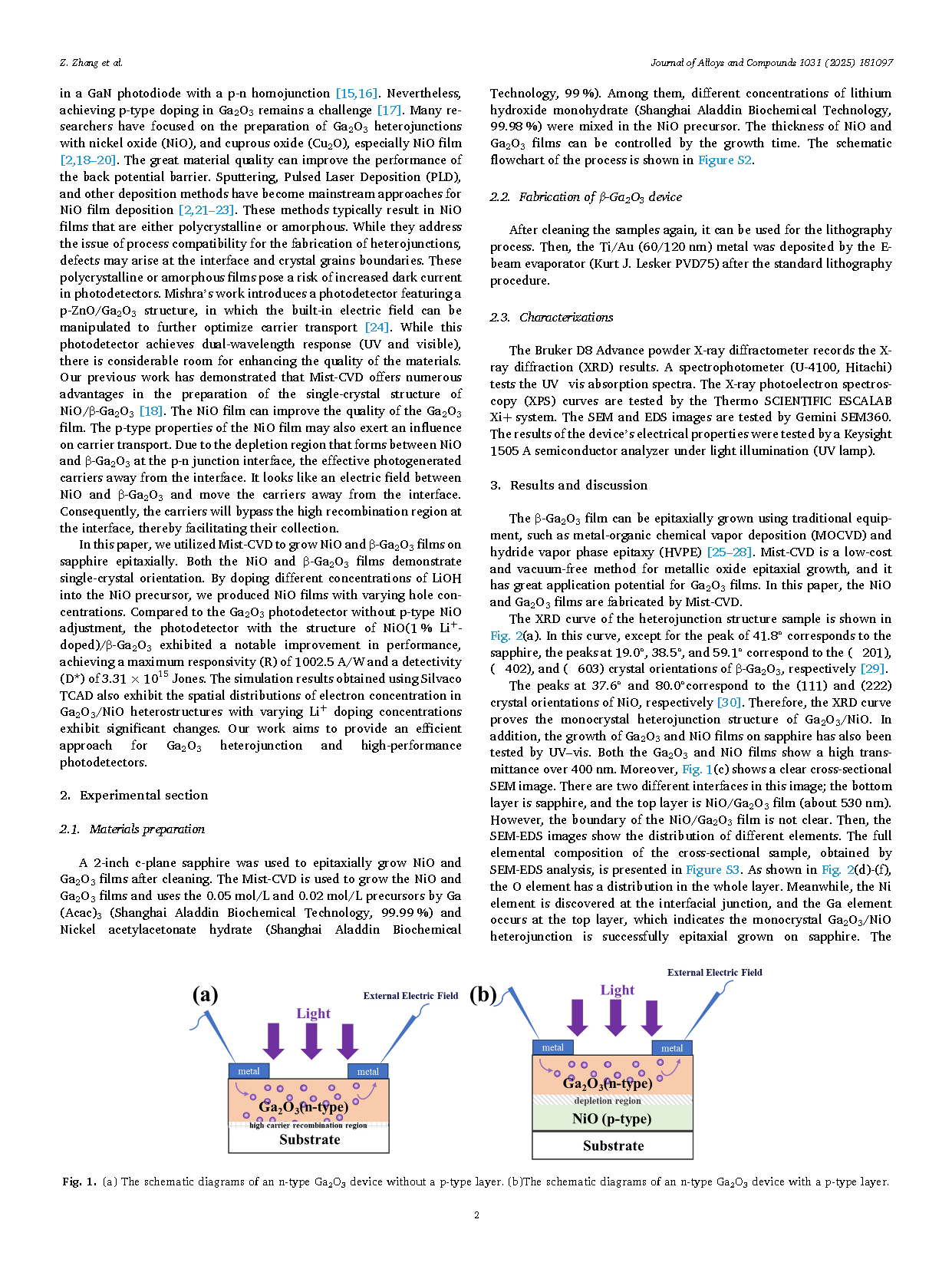
Fig. 2. (a) XRD curve of the heterojunction structure of Ga2O3/NiO/Sapphire. (b) The UV− vis transmittance spectra of Ga2O3 and NiO films on Sapphire. (c) The cross-sectional SEM image of the heterojunction with structure Ga2O3/NiO/Sapphire. (d)-(f) EDS mapping for Ni, Ga, and O elements, respectively.
DOI:
doi.org/10.1016/j.jallcom.2025.181097