Paper Sharing
【Member Papers】Xi'an University of Technology --- The impact of composite defects Vⁱₒ₍ɢₐ₎ on the electrical properties of β-Ga₂O₃/AlN heterojunctions
日期:2025-06-13阅读:741
Researchers from the Xi'an University of Technology have published a dissertation titled "The impact of composite defects ViO(Ga) on the electrical properties of β-Ga2O3/AlN heterojunctions" in Semiconductor Science and Technology.
Acknowledgment
This work was supported financially by the National Natural Science Foundation of China (Grant Nos. 62474139, 62104190, 61904146). This work was supported financially by Science and technology planning project of Xi’an (No. 2023JH-GXRC-0122), This work was supported financially by Natural Science Basic Research Program of Shaanxi (Program No. 2024JC-YBQN-0655). This work was supported financially by the Shaanxi Funds for Distinguished Young Scientists (2021JC-25).
Background
Ga2O3 exists in five distinct polymorphs: monoclinic (β-Ga2O3), rhombohedral (α), defective spinel (γ), cubic (δ), and orthorhombic (ε). Among them, β-Ga2O3 is the most stable and has been extensively researched. β-Ga2O3 exhibits an exceptionally wide bandgap (∼4.8 eV) and an extremely high critical breakdown field strength (∼8 MV cm−1) [1], bringing advantages such as high breakdown voltage and substantial output power. β-Ga2O3 exhibits a Baliga’s figure of merit 4 times higher than GaN, 10 times SiC, and 3444 times Si. This translates to lower on-resistance and reduced energy loss at the same operating voltage. Furthermore, the theoretical saturated electron velocity is approximately 2 × 107 cm s−1, rendering β-Ga2O3 highly suitable for high-frequency applications. Another major advantage of β-Ga2O3 is its ability to produce large-size intrinsic single-crystal substrates from the melt, and high-quality Ga2O3 epitaxial films of varying thicknesses can be easily grown using techniques such as metal–organic chemical vapor deposition (MOCVD), hydride vapor phase epitaxy, molecular beam epitaxy, and plasma-enhanced chemical vapor deposition. As a result, β-Ga2O3 has found extensive use in photodiodes, power diodes, metal-oxide-semiconductor field-effect transistors, and (AlxGa1-x)2O3/β-Ga2O3 MODFETs.
Conclusion
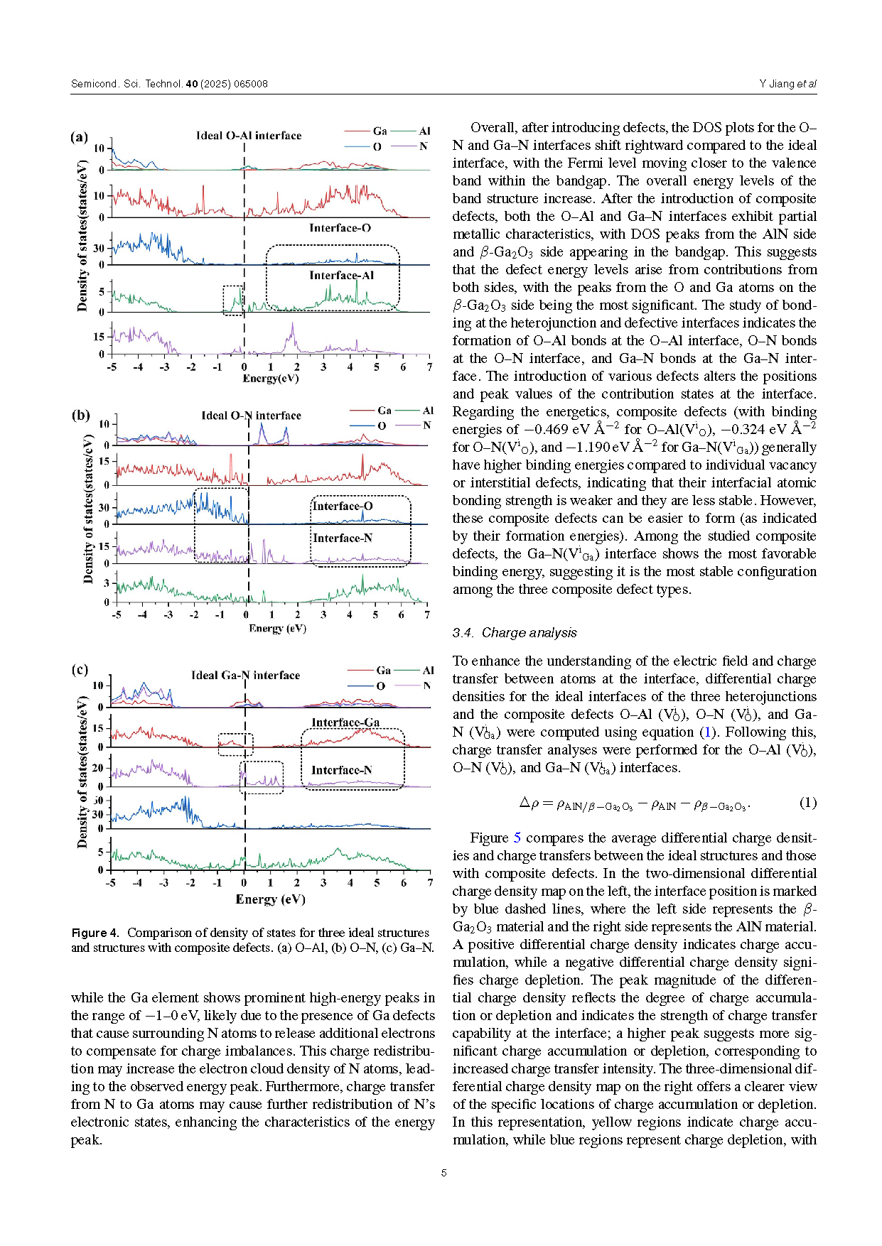
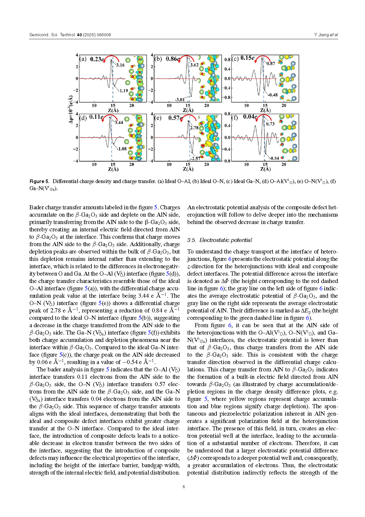
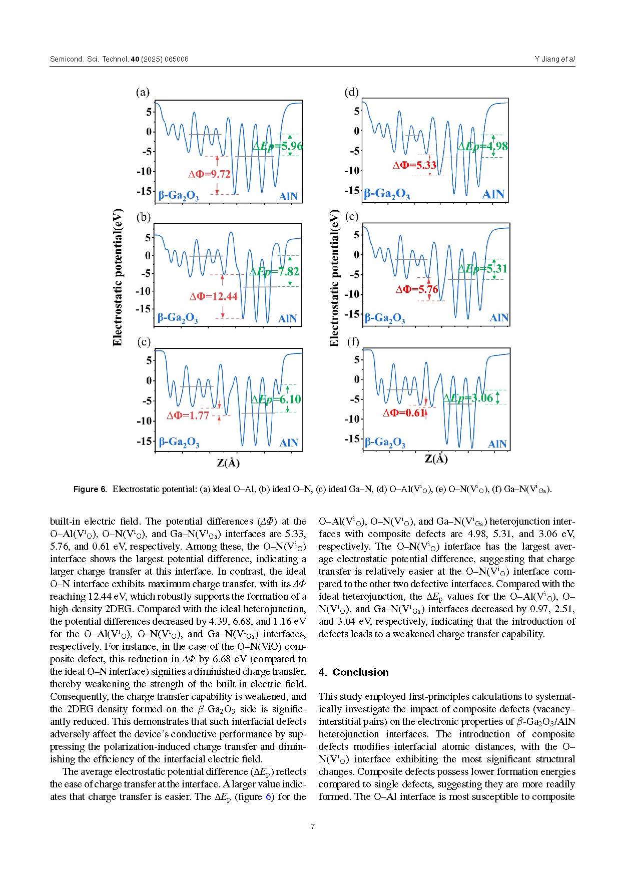
This study employed first-principles calculations to systematically investigate the impact of composite defects (vacancy– interstitial pairs) on the electronic properties of β-Ga2O3/AlN heterojunction interfaces. The introduction of composite defects modifies interfacial atomic distances, with the O–N(ViO) interface exhibiting the most significant structural changes. Composite defects possess lower formation energies compared to single defects, suggesting they are more readily formed. The O–Al interface is most susceptible to composite defect formation but exhibits poor stability, whereas the Ga–N interface forms the most stable composite defects, although their formation is the most energetically demanding. Composite defects induce partial metallicity at the O–Al and Ga–N interfaces. Defect states, primarily contributed by O and Ga atoms on the β-Ga2O3 side, appear within the bandgap, altering the energy positions and peak intensities of the interface states. Charge transfer from AlN to β-Ga2O3 is observed at all interfaces, resulting in an internal electric field pointing towards the Ga2O3 layer. The ideal O–N interface exhibits the strongest charge transfer, making it most conducive to forming a high-density 2DEG. While the presence of composite defects significantly reduces the magnitude of charge transfer, thereby weakening the internal electric field and diminishing the potential for high 2DEG density, the O–N(ViO) interface maintains the highest charge transfer among the defective interfaces studied. This research provides fundamental insights into the behavior of composite defects at β-Ga2O3/AlN heterojunction interfaces and their influence on electronic properties, offering valuable theoretical guidance for the design and optimization of high-performance electronic devices based on this heterostructure.

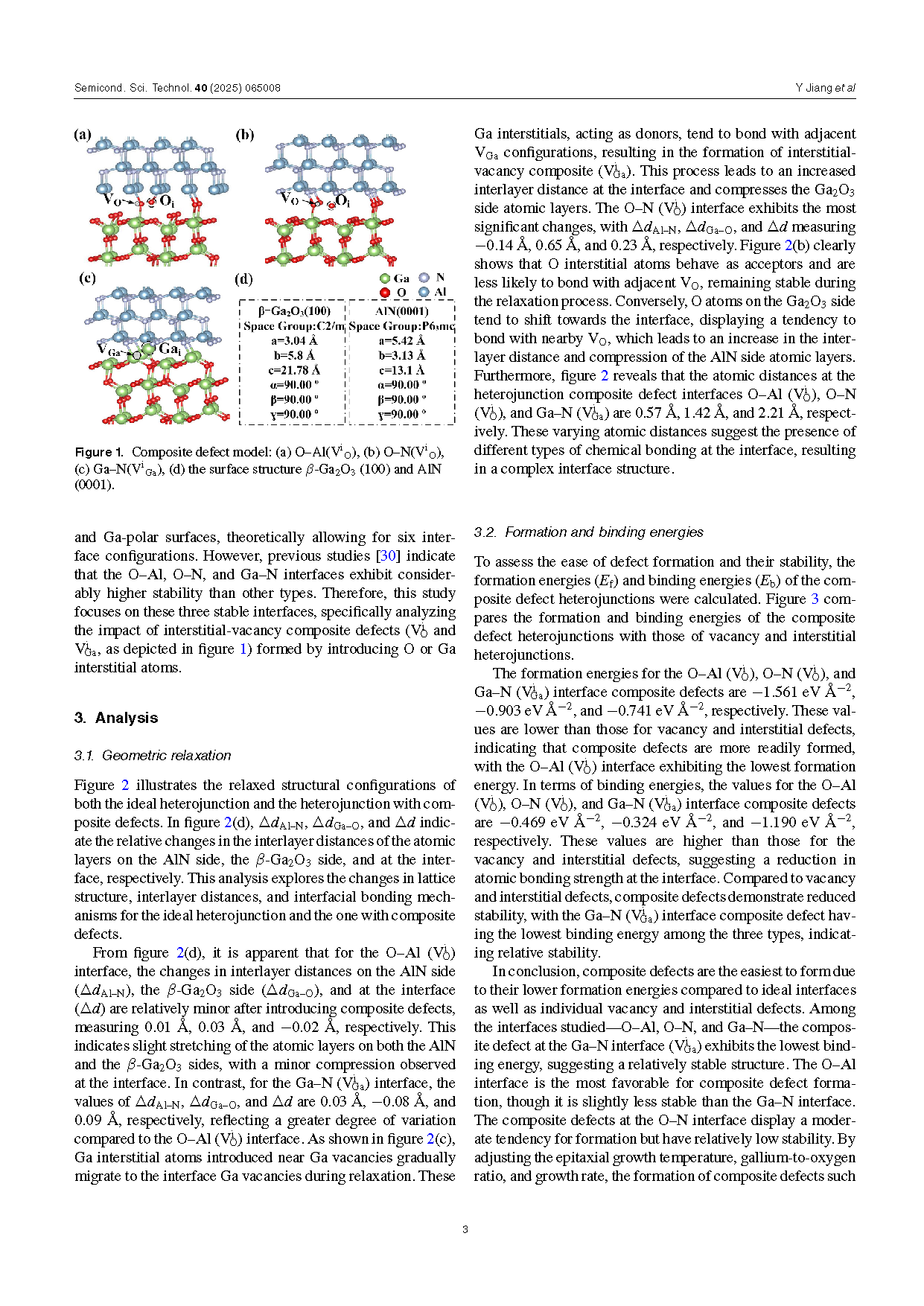
Figure 1. Composite defect model: (a) O–Al(ViO), (b) O–N(ViO), (c) Ga–N(ViGa), (d) the surface structure β-Ga2O3 (100) and AlN (0001).
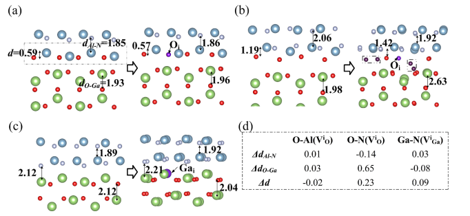
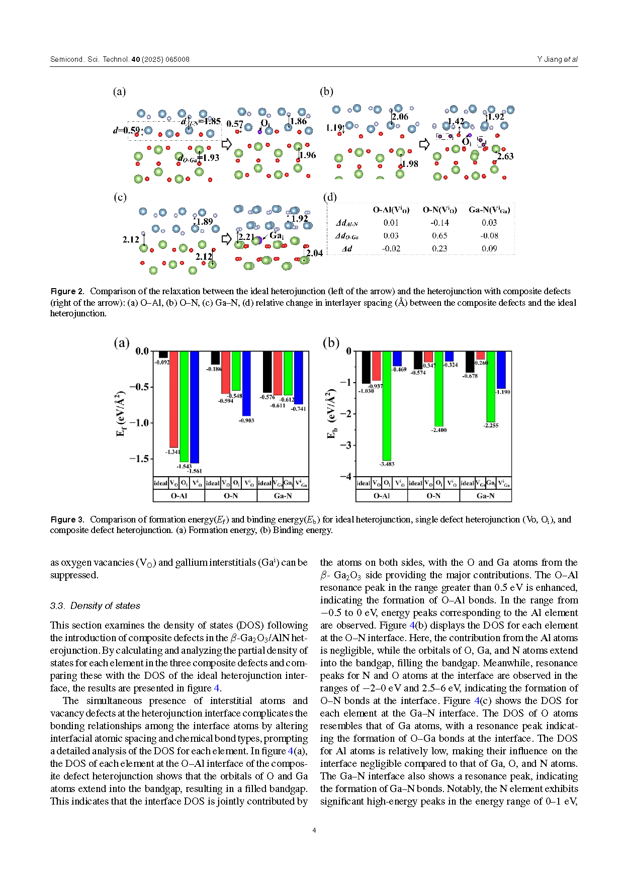
Figure 2. Comparison of the relaxation between the ideal heterojunction (left of the arrow) and the heterojunction with composite defects (right of the arrow): (a) O–Al, (b) O–N, (c) Ga–N, (d) relative change in interlayer spacing (Å) between the composite defects and the ideal heterojunction.
DOI:
doi.org/10.1088/1361-6641/addc14