


Paper Sharing
【Domestic Papers】University of Science and Technology of China---The mechanism of degradation and failure in NiO/β-Ga₂O₃ heterojunction diodes induced by the high-energy ion irradiation
日期:2025-06-13阅读:605
β -gallium oxide (β-Ga2O3) has a good application prospect in irradiation environments such as space systems with its ultra-wide band gap and high irradiation hardness. Among various irradiation effects, the single-particle effect often leads to transient failure of the device. Due to the low thermal conductivity and hole mobility, the single-particle effect of power devices based on β-Ga2O3 has been reported to be relatively serious, but at present, the reports of the single-particle effect are still relatively few. Meanwhile, the NiO/Ga2O3 heterojunction structure is an indispensable component of current β-Ga2O3 power devices. In response to the current lack of research on single-particle effects in β-Ga2O3 heterojunction devices, NiO/Ga2O3 heterojunction devices were fabricated and packaged to conduct single-particle effect experiments.
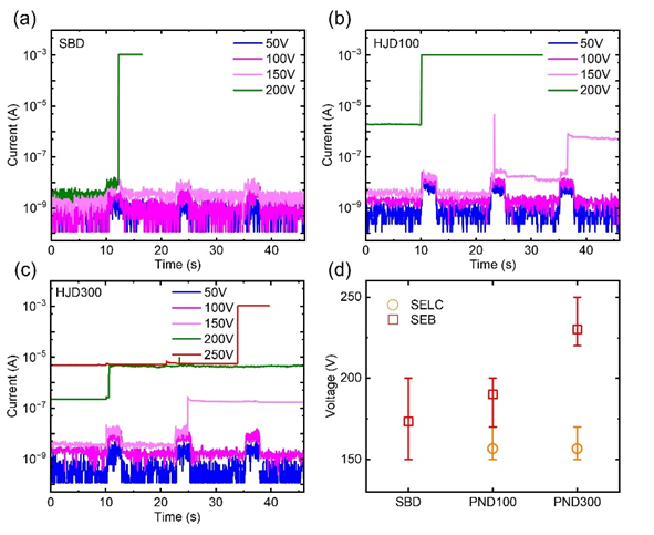
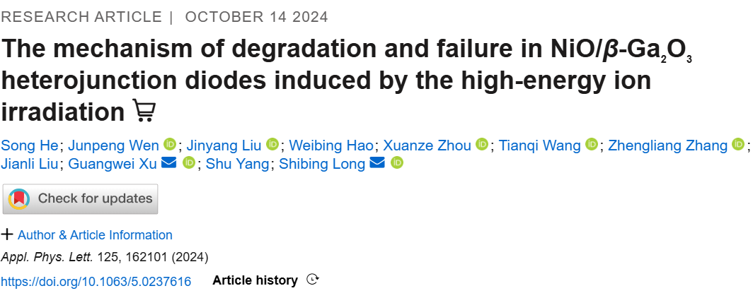
Figure 1. (a) β-Ga2O3 Schottky diode, (b) 100 nm, (b) 300 nm NiO heterojunction diode single-particle transient response. (d) Statistical distribution of SELC and SEB voltages for different types of devices.
This research group prepared Schottky diodes (SBD) for comparison and β-Ga2O3 heterojunction diodes (HJD) with different NiO thicknesses for single-event effect experiments on this issue. The experiment found that: Compared with SBD, the irradiation tolerance of HJD single particles is higher. After thickening NiO, the burnout voltage of single particles is further increased. Under different reverse biases, the single-particle transient response of the NiO/β-Ga2O3 heterojunction diode showed a trend of gradual current degradation (SELC) to final burnout (SEB), while surface electrode damage corresponding to current degradation and ablation holes corresponding to final failure were found on the surface of the burned device. Using a step gauge test, it was found that the surface electrode damage corresponded to the damage of the NiO and metal layers, while the ablation holes corresponded to perforations in the β-Ga2O3 epitaxial layer. The modeling of β-Ga2O3 heterojunction devices and the single-particle transient simulation show that the P-type region undertakes part of the space charge. Before irradiation, the peak electric field of the heterojunction device is relatively low. Therefore, the current, peak electric field and temperature responses under the single-particle transient are relatively low. When the NiO layer is thickened, the peak electric field is further reduced. However, due to the massive accumulation of non-equilibrium holes, both the intensity and range of the electric field in the NiO were significantly enhanced. Considering that the critical breakdown field strength of NiO is much lower than β-Ga2O3, it is theoretically speculated that the early breakdown of the NiO layer may be the cause of the degradation of the device, which is also consistent with the test results of the step meter.
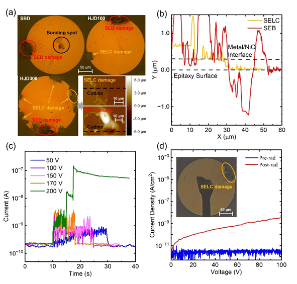
Figure 2. (a) Microscopic observation of the surface topography of the burned device, (b) step measurement of damage in the SELC and SEB regions. (c)(d) changes in leakage current of SELC but not SEB devices before and after irradiation.
Figure 3. (a)(d) β-Ga2O3 Schottky diode, (b)(e) 100 nm, (d)(f) 300 nm NiO heterojunction diode single-particle transient distribution of electric field and space charge.
Team Introduction
The National Science Fund for Distinguished Young Scholars led by Professor Long Shibing is based at the college of the University of Science and Technology of China. It has long been engaged in research in the fields of ultra-wide band gap semiconductor power devices, optoelectronic devices, and memory. The team, consisting of Distinguished Researcher Xu Guangwei, Distinguished Associate Researcher Zhao Xiaolong, postdoctoral Fellows Hou Xiaohu and Zhou Xuanze, and several doctoral students, is capable of conducting scientific research including material analysis, device fabrication, and circuit integration. The team has published many papers in international journals such as Nature Commu, Adv Marer, IEEE EDL, and in international conferences such as IEDM, ISPSD, and SISPAD.
DOI:
doi.org/10.1063/5.0237616
