


Paper Sharing
【Epitaxy Papers】LPCVD grown n-type doped β-Ga₂O₃ films on c-plane sapphire using TEOS precursor
日期:2025-06-13阅读:569
Researchers from the Indian Institute of Technology Kanpur have published a dissertation titled "LPCVD grown n-type doped β-Ga2O3 films on c-plane sapphire using TEOS precursor" in Materials Science in Semiconductor Processing.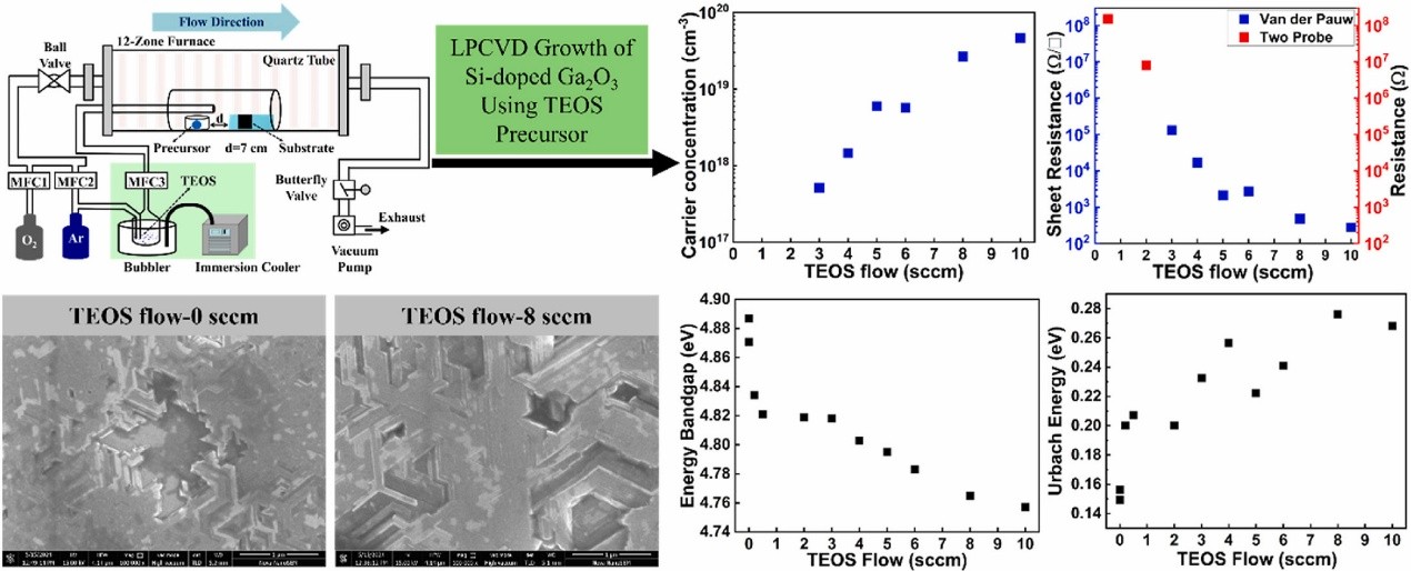
Abstract
β-Gallium Oxide (β-Ga2O3) is recognized as an ultrawide bandgap semiconductor material having large bandgap energy Eg = 4.4–4.9 eV. In addition to the high critical electric field of ∼7–8 MV/cm, it has an advantage of accessibility of melt-grown bulk substrates with large area. High-quality thin epitaxial films with precise carrier concentration control are pre-requisite to fabricate high-performance β-Ga2O3 devices. While n-type doping of β-Ga2O3 in LPCVD has been carried out with SiCl4 precursor and solid Ge, there are no reports of Si doping using organometallic dopant precursors such as Tetra-ethyl orthosilicate (TEOS) in LPCVD. In this study, we demonstrate controlled n-type doping of Ga2O3 heteroepitaxial films on c-plane sapphire using TEOS precursor as a source of Si dopant in an LPCVD system. By increasing the Ar flow through TEOS bubbler from 0.5 sccm to 10 sccm, resistance decrease of ∼6 orders is observed. Hall measurements conducted at room temperature reveal the carrier concentration increases from 5.14x10¹⁷– 4.65x1019 cm−3 as TEOS flow increases from 3 to 10 sccm, while an increase in mobility is observed from ∼2 cm2/V.s to ∼7 cm2/V.s before decreasing slightly at higher TEOS flow rates. Raman and XRD spectrum confirm the β-phase of Ga2O3 with (−201) orientation. Transmittance analysis showed an optical energy bandgap of 4.88 eV with no TEOS flow which gradually decreases to 4.75 eV as TEOS flow rate is increased to 10 sccm with a corresponding increase in the Urbach energy.
DOI:
https://doi.org/10.1016/j.mssp.2025.109697
