Paper Sharing
【Domestic Papers】National University of Defense Technology---Test on the Output Characteristics of Fe-β-Ga₂O₃ Photoconductive Semiconductor Device Toward High-Power Microwave Sources
日期:2025-06-11阅读:670
Researchers from the National University of Defense Technology have published a dissertation titled "Test on the Output Characteristics of Fe-β-Ga2O3 Photoconductive Semiconductor Device Toward High-Power Microwave Sources" in IEEE Transactions on Electron Devices.
Project support
This work was supported in part by the Key Program of the National Natural Science Foundation of China under Grant 62434010, in part by the National Natural Science Foundation of China under Grant 62101577, and in part by the Natural Science Foundation of Hunan Province under Grant 2025JJ20065.
Background
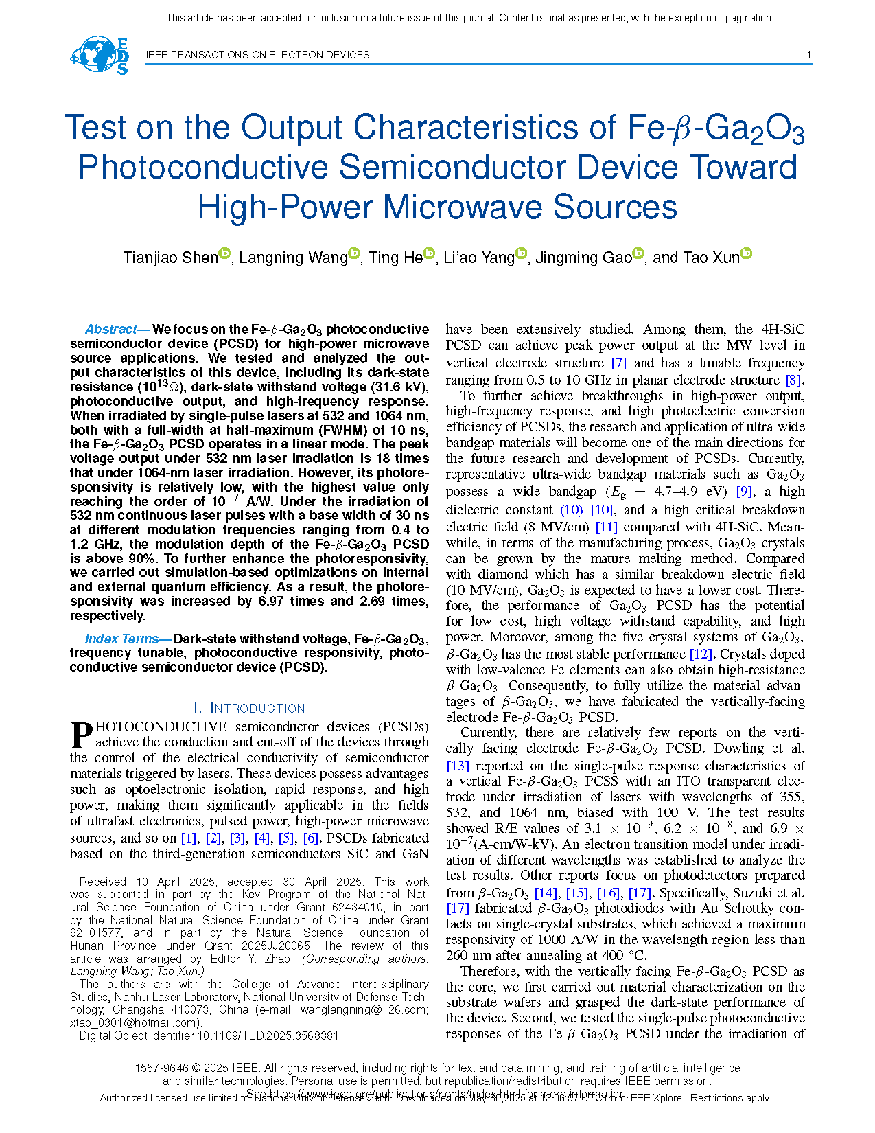
Photoconductive semiconductor devices (PCSDs) achieve the conduction and cut-off of the devices through the control of the electrical conductivity of semiconductor materials triggered by lasers. These devices possess advantages such as optoelectronic isolation, rapid response, and high power, making them significantly applicable in the fields of ultrafast electronics, pulsed power, high-power microwave sources, and so on. PSCDs fabricated based on the third-generation semiconductors SiC and GaN have been extensively studied. Among them, the 4H-SiC PCSD can achieve peak power output at the MW level in vertical electrode structure and has a tunable frequency ranging from 0.5 to 10 GHz in planar electrode structure. To further achieve breakthroughs in high-power output, high-frequency response, and high photoelectric conversion efficiency of PCSDs, the research and application of ultra-wide bandgap materials will become one of the main directions for the future research and development of PCSDs. Currently, representative ultra-wide bandgap materials such as Ga2O3 possess a wide bandgap (Eg = 4.7–4.9 eV), a high dielectric constant, and a high critical breakdown electric field (8 MV/cm) compared with 4H-SiC. Meanwhile, in terms of the manufacturing process, Ga2O3 crystals can be grown by the mature melting method. Compared with diamond which has a similar breakdown electric field (10 MV/cm), Ga2O3 is expected to have a lower cost. Therefore, the performance of Ga2O3 PCSD has the potential for low cost, high voltage withstand capability, and high power. Moreover, among the five crystal systems of Ga2O3, β-Ga2O3 has the most stable performance. Crystals doped with low-valence Fe elements can also obtain high-resistance β-Ga2O3. Consequently, to fully utilize the material advantages of β-Ga2O3, we have fabricated the vertically-facing electrode Fe-β-Ga2O3 PCSD.
Abstract
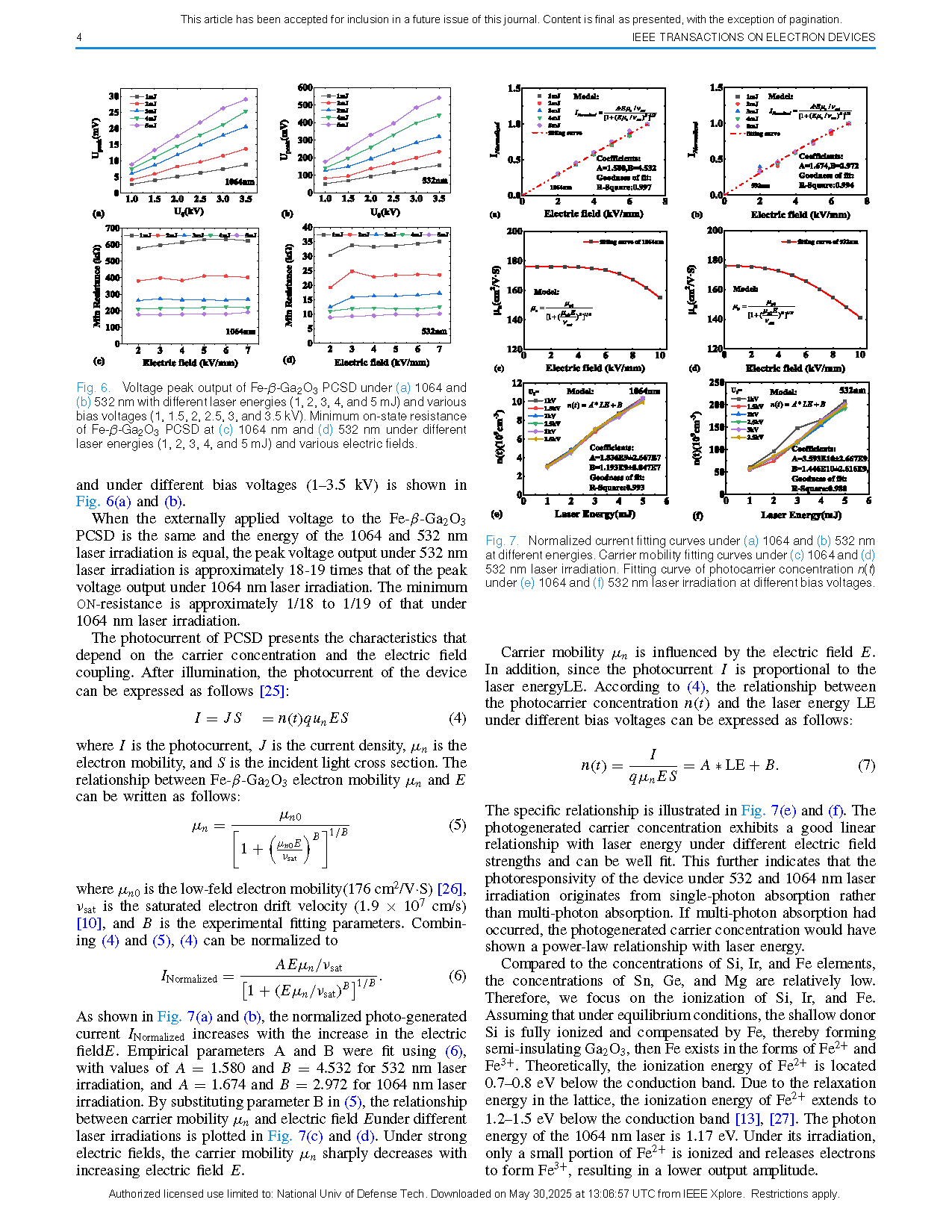
We focus on the Fe-β-Ga2O3 photoconductive semiconductor device (PCSD) for high-power microwave source applications. We tested and analyzed the output characteristics of this device, including its dark-state resistance (1013Ω), dark-state withstand voltage (31.6 kV), photoconductive output, and high-frequency response. When irradiated by single-pulse lasers at 532 and 1064 nm, both with a full-width at half-maximum (FWHM) of 10 ns, the Fe-β-Ga2O3 PCSD operates in a linear mode. The peak voltage output under 532 nm laser irradiation is 18 times that under 1064-nm laser irradiation. However, its photoresponsivity is relatively low, with the highest value only reaching the order of 10-7 A/W. Under the irradiation of 532 nm continuous laser pulses with a base width of 30 ns at different modulation frequencies ranging from 0.4 to 1.2 GHz, the modulation depth of the Fe-β-Ga2O3 PCSD is above 90%. To further enhance the photoresponsivity, we carried out simulation-based optimizations on internal and external quantum efficiency. As a result, the photoresponsivity was increased by 6.97 times and 2.69 times, respectively.
Conclusion
A vertically-electrode-configured Fe-β-Ga2O3 PCSD device was designed and tested to evaluate its output performance.
1) Thanks to the wide bandgap of gallium oxide, the Fe-β-Ga2O3 PCSD can withstand a dark voltage of 31.5 kV. The field concentration effect at the triple junction of the device leads to bulk breakdown at the edges of the electrodes.
2) Based on single-pulse test results, a model was established to describe the relationship between the internal mobility and photogenerated carrier concentration of the device and the electric field and laser energy. This model confirmed the single-photon linear absorption behavior of the device under 1064 and 532 nm laser triggering.
3) In addition, the device demonstrates a modulation depth of over 90% for microwaves at 1.2 GHz.
In future work, we will consider using lasers with shorter wavelengths to test the optoelectronic response of the device and focus on optimizing the doping concentration of Fe-β-Ga2O3 PCSD and the reflective optical path, thereby laying the foundation for achieving higher output power and higher response frequencies in Fe-β-Ga2O3 PCSD.
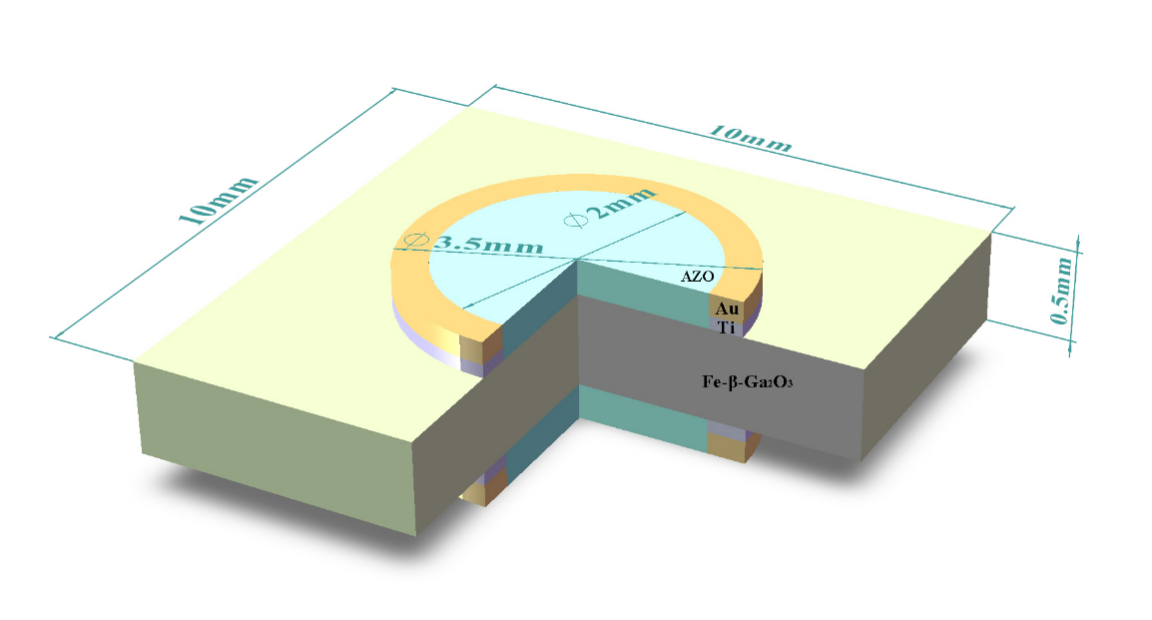
Fig. 1. Structure of the perpendicular normal-incidence Fe-β-Ga2O3 PCSD.
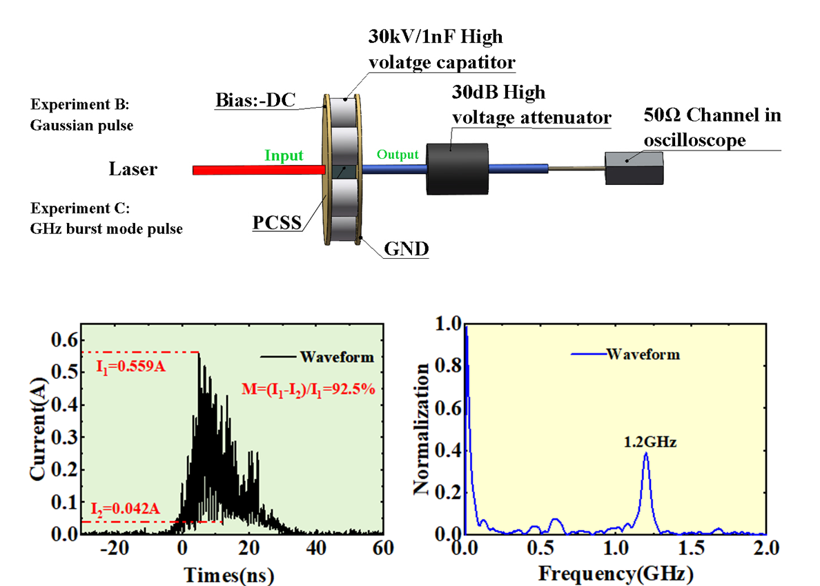
Figure 2. Schematic diagram of the laser illumination test link and the frequency response result at 1.2 GHz
DOI:
doi.org/10.1109/TED.2025.3568381