


Discover
【Knowledge Discover】Proposal and Working Principle of Gallium Oxide p-NiO Heterojunction Bidirectional Switching Device
日期:2025-06-06阅读:2126
(This article is reposted from a personal WeChat offical account.)
A while ago, we talked about "Power P-GaN SJ BDS- Gallium Nitride super-junction withstand voltage bidirectional switching device ", concentrating all the surge electrical stresses of the original transverse PSJ and transverse p-GaN ReSURF on the line closest to the edge of the polarization structure.
There are problems with overload surge reliability, and the large capacitance of the ReSURF field plate makes the problem of thermal electron injection in this area of overload surge even more severe. So author thought for a moment. Why not make it a p-GaN thin layer with multiple similar field-limiting loops, all connected to the drain at the same time, to form a RESURF super-junction withstand voltage structure with uniform voltage division and simultaneous consideration?
Let's try making another bidirectional withstand voltage switch?
But what is the name? Power P-GaN SJ BDS- Gallium Nitride super-junction withstand voltage Bidirectional Switching Device?
A friend left a message asking me, "Author, aren't you going to share and discuss the new device structure of Gallium Oxide?" Can the SJ BDS construction of this super-junction bidirectional switching device be used in Gallium Oxide devices?
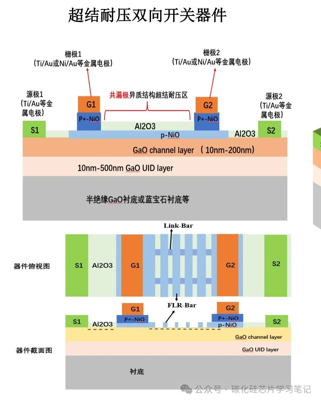
Of course, Author would like to give it a try. If one day have A second Shuji Nakamura discovers a new buffer growth technique that can be used on silicon/sapphire wafers... Gallium Oxide epitaxial layers of single crystal quality and quasi-single crystal quality are directly grown on different substrates. Then, perhaps in the future, Gallium Oxide materials will shine brightly, truly shining in the field of heterogeneous epitaxial transverse high-voltage devices, and even in the field of high-voltage integrated ics, and even replacing GaN or Silicon Carbide devices in many fields?
Let's ask Deepseek...
The heterojunction bidirectional switching device composed of Gallium Oxide (Ga₂O₃) and P-type Nickel Oxide (p-NiO) is a new type of power electronic device. Its working principle combines the characteristics of wide band gap semiconductor materials, heterojunction band engineering and superjunction structure design to achieve high withstand voltage, low loss and bidirectional controllable switching functions. Here is a detailed analysis of how it works:
### **1. Material and Structural Properties **
- **Gallium Oxide (Ga₂O₃) ** :
- Ultra-wide band gap semiconductor (bandgap approximately 4.8-4.9 eV), with an extremely high critical breakdown electric field (about 8 MV/cm), suitable for high-voltage applications.
- Naturally N-type conductive but lacking stable P-type doping, P-type materials (such as p-NiO) need to be introduced through heterojunctions.
- ** P-Type Nickel Oxide (p-NiO) ** :
- A P-type transparent conductive oxide that forms a heterojunction with Ga₂O₃, compensates for the P-type defect of Ga₂O₃, and provides hole injection capability.
- Band alignment at the heterojunction interface is crucial for carrier transport (may form Type-II band structures that facilitate charge separation).
- ** Superjunction Structure ** :
- Composed of alternating p-NiO and n-Ga₂O₃ regions, it optimizes the transverse electric field distribution through charge balance, significantly boosting breakdown voltage while reducing on-resistance.
---
### **2. Bidirectional Switching Mechanism **
** (1) Blocking State (off state) **- *
* forward and reverse blocking ** :
- Under bidirectional voltage, the heterojunction interface and the superjunction structure extend the uniformly distributed electric field through the depletion region to avoid local electric field concentration.
- The charge balance of the superjunction causes the longitudinal electric field (perpendicular to the junction direction) to be shared by the transverse electric field (parallel to the junction direction), significantly increasing the breakdown voltage (up to thousands of volts).
** (2) Conduction State (Open state) **
- ** Bidirectional Carrier Injection ** :
- ** Forward Bias (Ga₂O₃ terminal positive) ** :
Holes of p-NiO are injected into Ga₂O₃, electrons of Ga₂O₃ are injected into p-NiO, the heterojunction barrier is lowered, and bipolar conduction is formed.
- Reverse bias (Ga₂O₃ terminal connected to negative) :
Through the symmetrical design of the superjunction structure, the p-NiO and Ga₂O₃ interfaces also form conduction paths under reverse bias, enabling bidirectional current flow.
- The high doping concentration of the superjunction structure further reduces the on-resistance (Ron) and improves efficiency.
** (3) Switching Trigger Mechanism **
- ** Voltage Trigger ** :
- When the applied voltage exceeds the threshold, avalanche breakdown or tunneling occurs in the heterojunction depletion region, causing carrier doubling and rapid conduction of the device.
- ** Field Control Effect ** :
- Active switching control is achieved by regulating the height of the heterojunction barrier through the gate (if designed) or structural electric field.
---
### **3. Key Advantages **- *
-** High Withstand Voltage Capability ** : The superjunction structure and the high breakdown field strength of Ga₂O₃ work together to support several kilovolt-level blocking voltages. - ** Low Conduction Loss ** : Bipolar conduction mechanism (where both electrons and holes are involved in conduction) reduces Ron and improves energy efficiency.
- ** Bidirectional Symmetry ** : Structural design ensures consistent electrical properties in both forward and reverse directions, suitable for AC circuits or bidirectional power control.
- ** High-Temperature Stability ** : The wide band gap material is resistant to high temperatures and suitable for applications in harsh environments.
---
### **4. Potential Applications **
-** High-Voltage DC/AC Converters ** : such as smart grids, electric vehicle charging systems.
- ** Solid-State Circuit Breaker ** : Fast-response, highly reliable circuit protection.
- ** RF Power Devices ** : High frequency, high power communication systems.
---
### 5. Challenges and Research Directions **
-** Interface Optimization ** : The interface defect of Ga₂O₃/p-NiO heterojunctions may affect carrier transport and need to be improved through annealing or interface passivation.
- ** Thermal Management ** : Ga₂O₃ has a low thermal conductivity and requires the integration of heat dissipation design (such as diamond substrate integration).
- ** Process Compatibility ** : Heteroepitaxial growth and superjunction manufacturing have higher process complexity and require the development of low-cost mass production technology.
---
### ** Summary
The Gallium Oxide /p-NiO heterojunction bidirectional switching device achieves high-voltage bidirectional conduction and fast switching characteristics through the synergy of heterojunction band engineering and superjunction charge balance design. It is expected to break through the performance limit of traditional silicon-based devices and promote the development of the next generation of high-power electronic systems.
