Paper Sharing
【Member Papers】Xidian University --- Double-pulsed-induced medium-range order in Sn-doped Ga₂O₃ thin films: A strategy for enhanced record-breaking electrical properties
日期:2025-06-06阅读:868
Researchers from the Xidian University have published a dissertation titled "Double-pulsed-induced medium-range order in Sn-doped Ga2O3 thin films: A strategy for enhanced record-breaking electrical properties" in Applied Physics Letters.
Project support
This work was supported by the National Natural Science Foundation of China (NSFC) under Grant No. U21A20503.
Background
As the applications of wide-bandgap semiconductor materials in power electronics and optoelectronic devices continue to grow, gallium oxide (Ga2O3) has attracted considerable attention due to its outstanding physical and electrical properties. With a wide bandgap of approximately 4.9 eV, Ga2O3 offers exceptional stability under high-temperature and high-electric field conditions, as well as low leakage current, making it an ideal candidate for next-generation, high-performance electronic devices. Nonetheless, in practical scenarios, the intrinsic carrier concentration of pure Ga2O3 films remains relatively low, which limits their conductivity and prevents them from fulfilling the demands of high-efficiency power devices. As a result, the development of effective doping strategies to enhance both the carrier concentration and mobility of Ga2O3 films has become a central focus of contemporary research. To improve the material’s conductivity, n-type doping—particularly with elements such as Sn and Si—has been extensively studied, with Sn doping standing out due to its significant impact on carrier concentration. However, traditional deposition methods often introduce lattice defects and lead to disordered doping, which, in turn, can cause increased carrier scattering and reduced mobility, ultimately negating the conductivity improvements achieved through doping. Consequently, one of the key challenges in enhancing the electrical properties of Ga2O3 films lies in introducing dopants without compromising the films’ crystalline quality and chemical uniformity.
Abstract
This study explores Sn-doped Ga2O3 thin films synthesized via the double-pulse metalorganic chemical vapor deposition (MOCVD) method, highlighting its unique advantages in improving film microstructure and electrical properties. The results show that the double-pulse Sn-doped technique, through intermittent atomic supply, promotes medium-range ordering of Sn atoms within the Ga2O3 lattice, reducing lattice defects and enhancing crystallinity. Secondary ion mass spectrometry further reveals a doping activation rate of 95%. Notably, the films exhibit exceptional electrical performance, achieving a Hall mobility of 175.61 cm2/V·s at a carrier concentration of 2.17 × 1018 cm−3. This value represents a record-high mobility for β-Ga2O3 at this carrier concentration, significantly surpassing the performance of films prepared via conventional continuous deposition methods. This study offers valuable insights into the mechanisms of double-pulse MOCVD and its potential for Ga2O3-based high-performance electronic devices, providing an effective pathway for optimizing next-generation electronic materials.
Conclusion
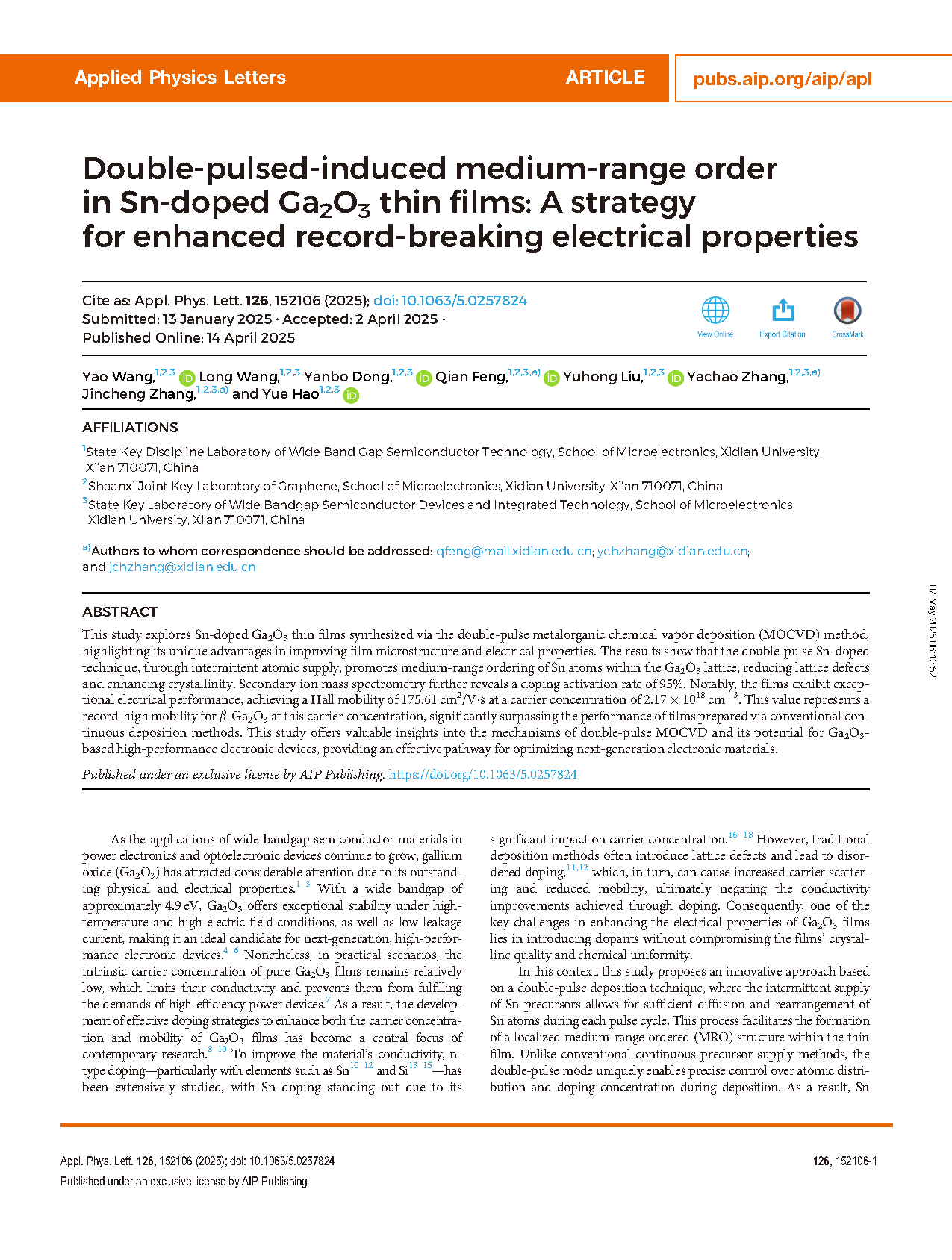
To summarize, we have systematically analyzed the remarkable optimization of both the microstructure and electrical properties of Sn-doped Ga2O3 thin films through the double-pulse MOCVD technique. The intermittent nature of the double-pulse deposition process, where atomic supply is precisely controlled during each deposition pulse and pause, plays a crucial role in promoting MRO of Sn atoms within the Ga2O3 lattice at the nanoscale. This localized ordering enhances the carrier mobility and doping activation, leading to a significant improvement in the electrical properties of the films. Specifically, the Hall mobility of the films deposited with the double-pulse technique reached an impressive 175.61 cm2/V·s, accompanied by a carrier concentration of 2.17 × 1018 cm−3. Moreover, the combination of SIMS and Hall test results demonstrated that the doping activation efficiency under this deposition mode reached as high as 95%, highlighting the technique’s effectiveness in enhancing doping efficiency and optimizing the film’s conductivity. This breakthrough provides a valuable foundation for the development of high-performance Ga2O3-based electronic devices, offering a promising approach for the fabrication of advanced doped oxide semiconductors that could have significant applications in future electronic and optoelectronic devices.
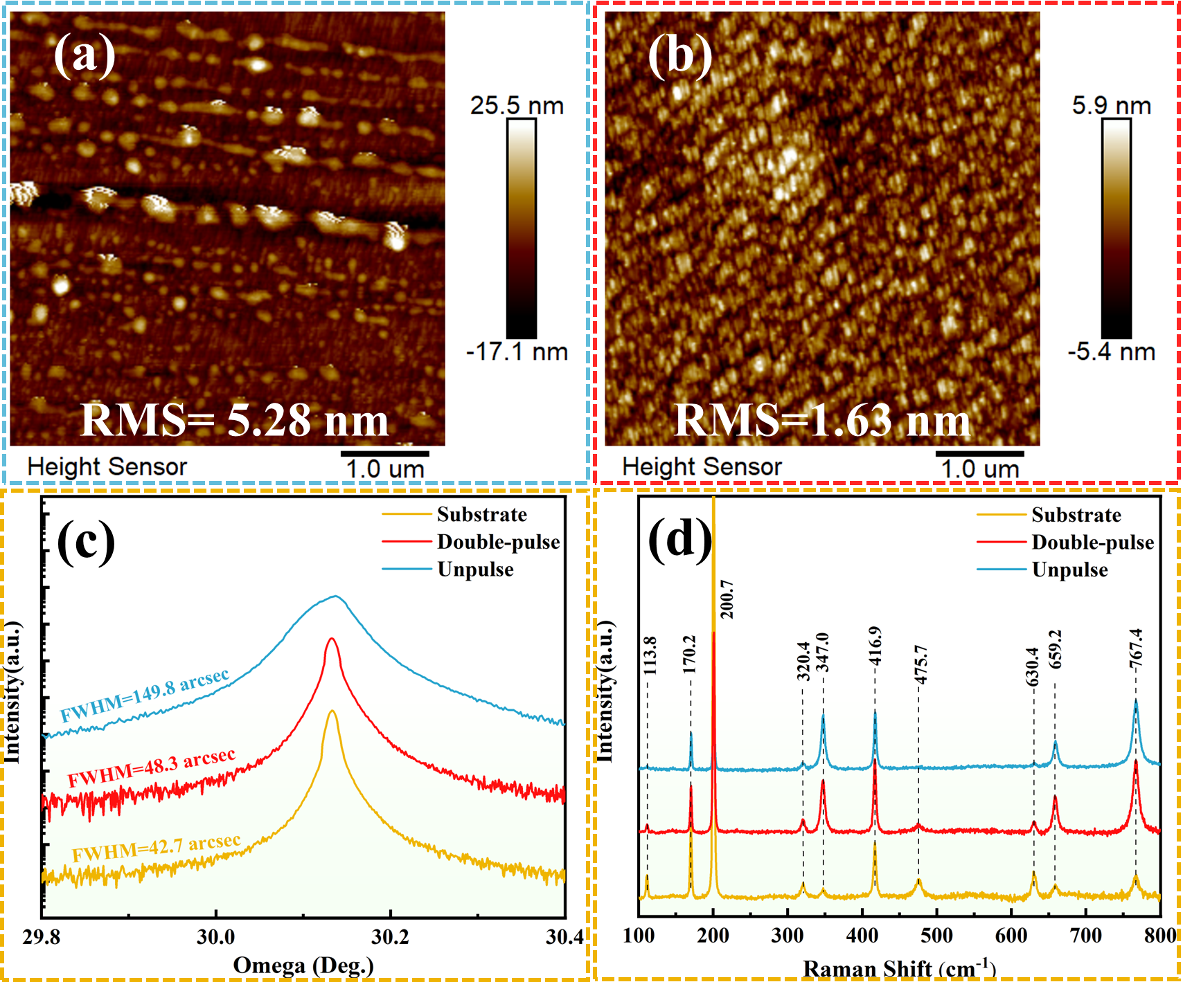
图1. (a) 和 (b) 分别显示了未脉冲和双脉冲样品的AFM表面形态图像;(c) 和 (d) 展示了衬底、未脉冲和双脉冲样品的XRD图和拉曼光谱。
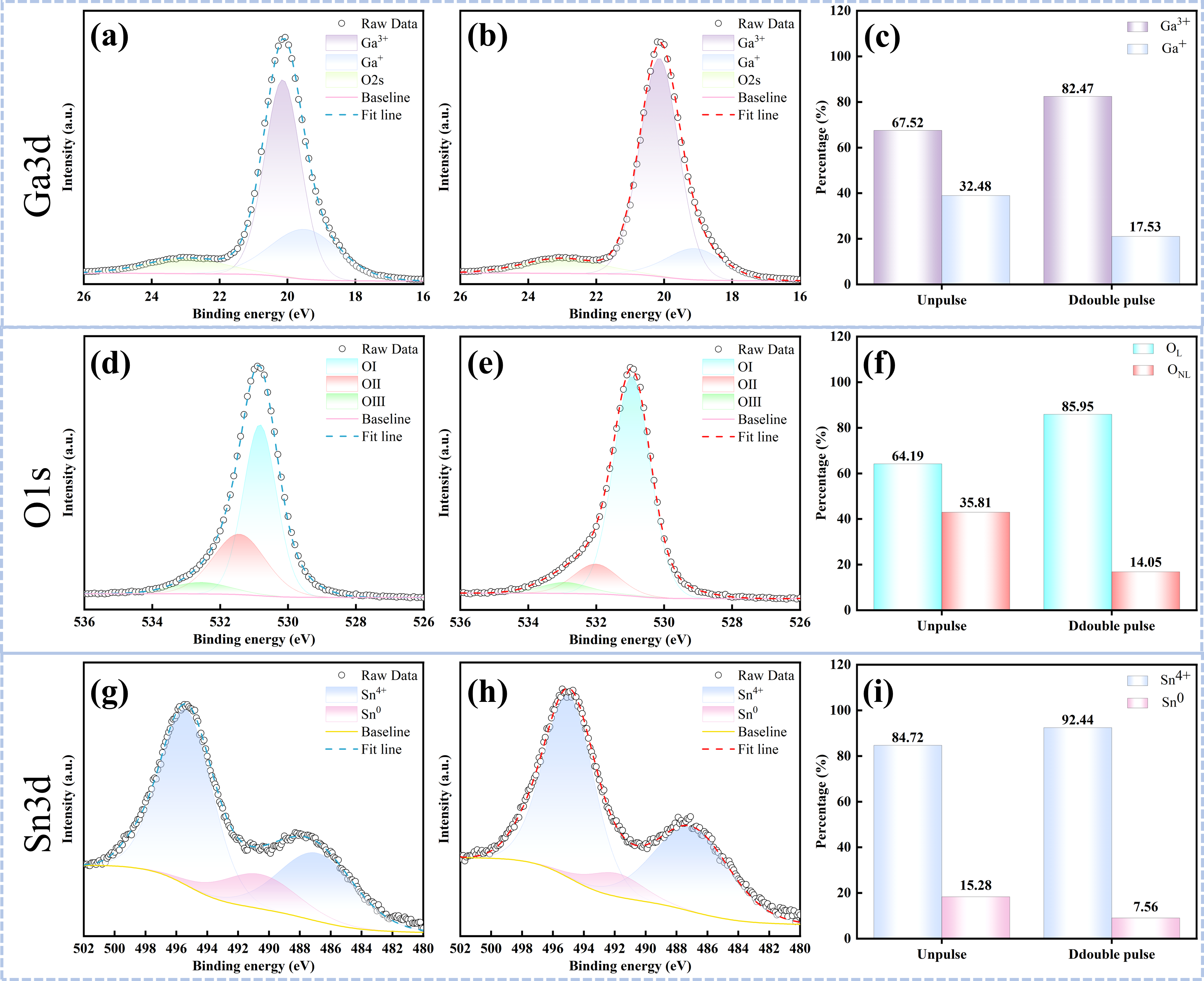
图2. β-Ga2O3 薄膜的 XPS 核心能级光谱:(a)和(b)Ga 3d。(c)Ga3+ 和 Ga+ 的百分比。(d)和(e)O 1s。(f)晶格氧和非晶格氧的百分比。(g)和(h)Sn 3d。(i)Sn4+ 和 Sn0 的百分比。
DOI:
doi.org/10.1063/5.0257824