Paper Sharing
【International Papers】Fabrication of air bridges on (100) β-Ga₂O₃ using crystallographic HCl gas etching
日期:2025-06-06阅读:804
Researchers from the National Institute for Materials Science have published a dissertation titled "Fabrication of air bridges on (100) β-Ga2O3 using crystallographic HCl gas etching" in AIP Advances.
Background
In recent years, β-Ga2O3 has emerged as a promising ultra-wide bandgap semiconductor. As β-Ga2O3 has a bandgap of 4.43 eV, its Baliga’s figure of merit surpasses those of traditional wide bandgap materials such as SiC and GaN and makes it an excellent candidate for power device applications. Because of its corresponding optical absorption edge at 280 nm, β-Ga2O3 exhibits native solar-blind sensitivity without bandgap tuning, making it a suitable material for solar-blind and flame detectors. In addition, as β-Ga2O3 responses to reducing and oxidizing gases, it is applicable to gas sensors. Furthermore, large β-Ga2O3 bulk single crystals with controlled conductivity can be grown with the use of melt growth techniques. This makes it possible to produce low-cost, high-crystalline wafers and substrates for device fabrication. These advantages have driven the rapid progress in the research and development of β-Ga2O3-based devices and have led to the realization of high-performance devices.
Along with its electrical, optical, and gas-sensing advantages, β-Ga2O3 is characterized by excellent mechanical properties, including a relatively high Young’s modulus of ∼261 GPa and an acoustic velocity of ∼6623 m s−1, which make it well-suited to micro-electromechanical systems (MEMS). Through the integration of their electrical, optical, chemical sensing, and mechanical properties, β-Ga2O3 MEMS components are particularly valuable in high-power, high-frequency devices and resonance-enabled solar-blind ultraviolet photodetectors and gas sensors. Recent advances in β-Ga2O3-based MEMS highlight the material potentials in high-frequency resonators, vibrating channel transistors, and resonant UV and gas sensors.
Abstract
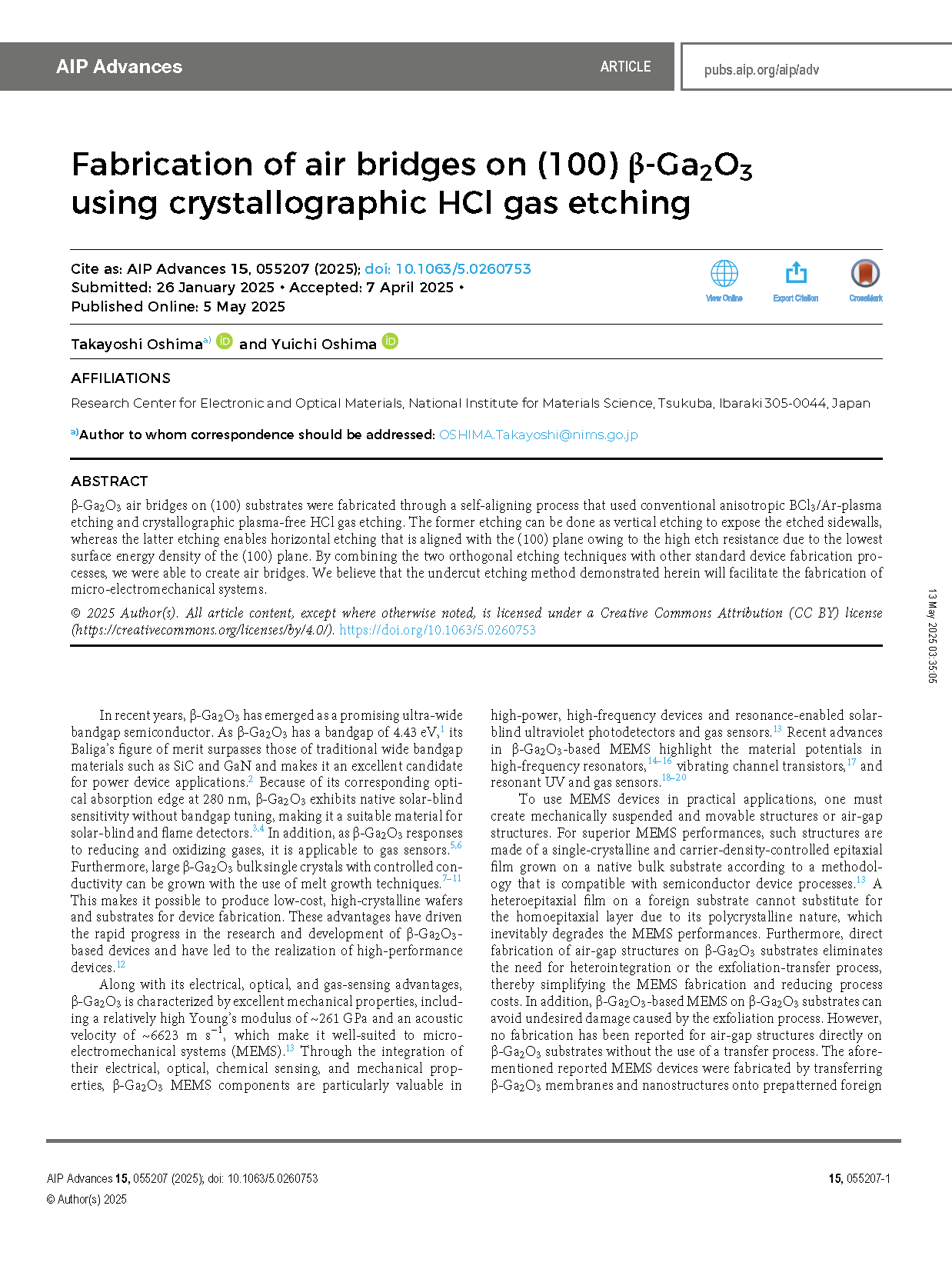
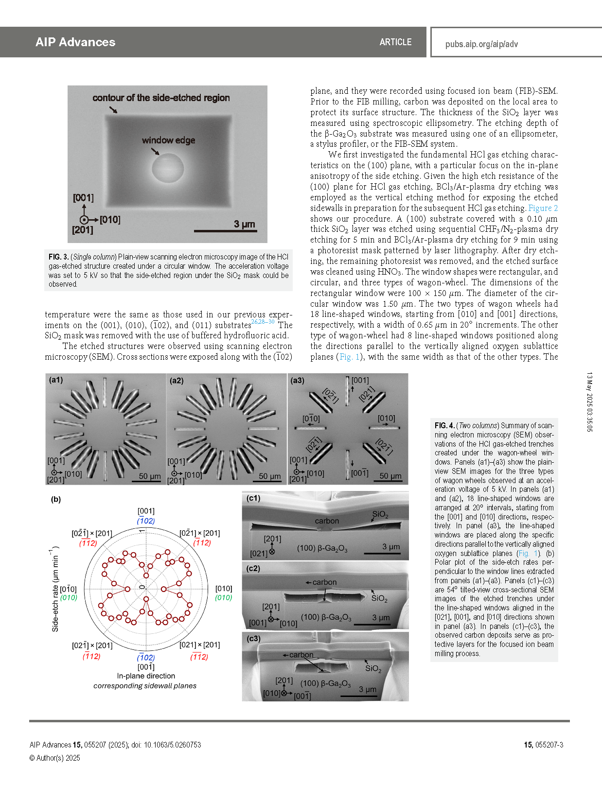
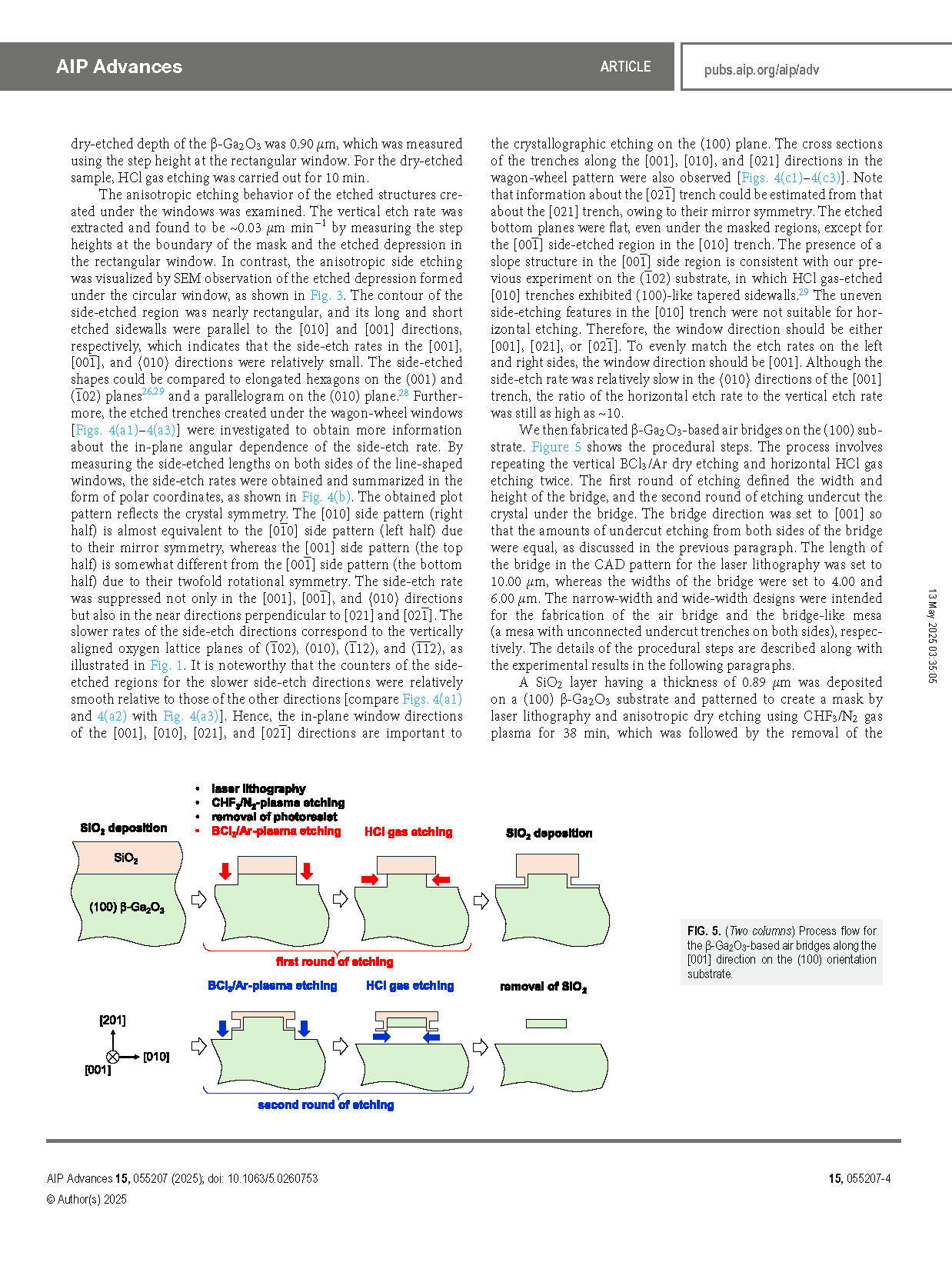
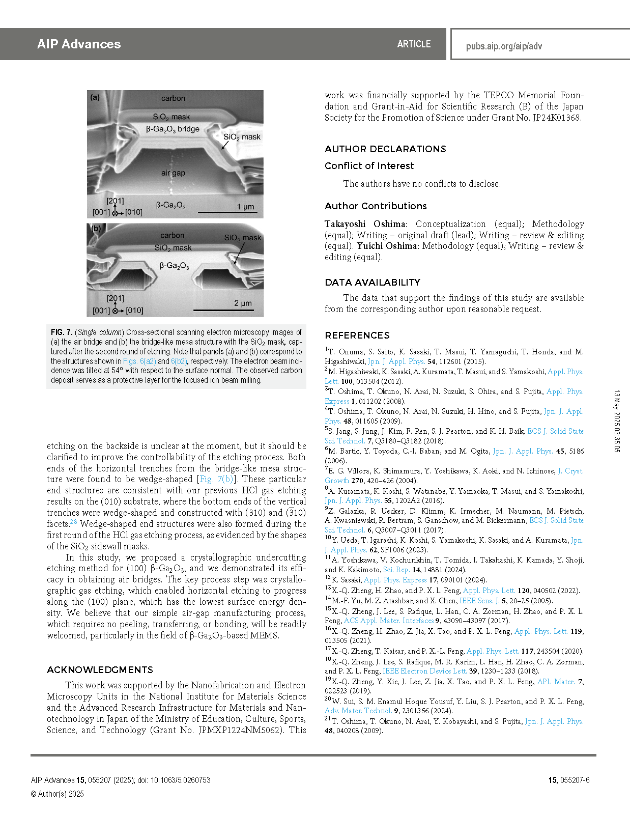
β-Ga2O3 air bridges on (100) substrates were fabricated through a self-aligning process that used conventional anisotropic BCl3/Ar-plasma etching and crystallographic plasma-free HCl gas etching. The former etching can be done as vertical etching to expose the etched sidewalls, whereas the latter etching enables horizontal etching that is aligned with the (100) plane owing to the high etch resistance due to the lowest surface energy density of the (100) plane. By combining the two orthogonal etching techniques with other standard device fabrication processes, we were able to create air bridges. We believe that the undercut etching method demonstrated herein will facilitate the fabrication of micro-electromechanical systems.
Graphic Examples

FIG. 1. Atomic arrangement of the β-Ga2O3 structure projected along the [201] direction normal to the (100) plane. Low Miller index, oxygen sublattice planes vertical to the (100) plane, and the corresponding in-plane directions are also indicated.
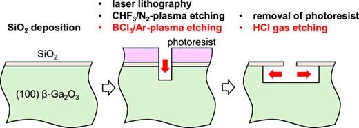
FIG. 2. Process flow for the horizontal etching on the substrate with (100) orientation.
DOI:
doi.org/10.1063/5.0260753