Paper Sharing
【International Papers】Self-powered NiO/κ-Ga₂O₃ heterojunction photodiode for fast broadband ultraviolet (UV) radiation detection
日期:2025-05-29阅读:1039
Researchers from the University of Parma have published a dissertation titled "Self-powered NiO/κ-Ga2O3 heterojunction photodiode for fast broadband ultraviolet (UV) radiation detection" in Optical Materials.
Project Support
This work was supported by the Italian National Recovery and Resilience Plan (PNRR), Mission 4, Component 2, funded by NextGenerationEU: Project “Ecosystem for Sustainable Transition in Emilia-Romagna - (Ecosister)”, Code ECS00000033; PRIN Project “UV-C Sensors based on Gallium Oxide (USE GAO)”, Code 2022A4AN2F; and by Project “MUR_DM737_A_MAFI_PARISINI DM 737 - 25.06.2021 - Ga2O3-based diodes for power electronics”.
Background
Current commercial ultraviolet (UV) detectors are typically designed to detect broadband UV radiation encompassing the UVA, UVB, and UVC regions and to operate with low power consumption. However, these detectors, particularly those utilizing narrow bandgap materials, tend to absorb visible light, reducing UV selectivity, and require optical filters. Broadband UV detectors must detect light photons in a very wide spectral range including the UVA (315 nm < λ < 400 nm), UVB (280 nm < λ < 315 nm), and UVC (100 nm < λ < 280 nm) regions. These devices offer significant advantages over single-wavelength UV detectors (selective detectors) as they enable the simultaneous detection of different UV-light wavelengths, which is crucial in a wide range of applications including advanced communication systems, space applications, flame detection and ozone sensing. UV detectors have undergone significant advancements over the past decade, driven by continuous innovations in semiconductor materials and device manufacturing processes. These advancements have paved the way to the successful fabrication of "single-band (selective)" and “dual-band” UV detectors. However, the fabrication of devices working over the entire UV wavelength range, while maintaining high responsivity and detectivity, short response and recovery times, ability to operate remotely without power supply remains a technological challenge.
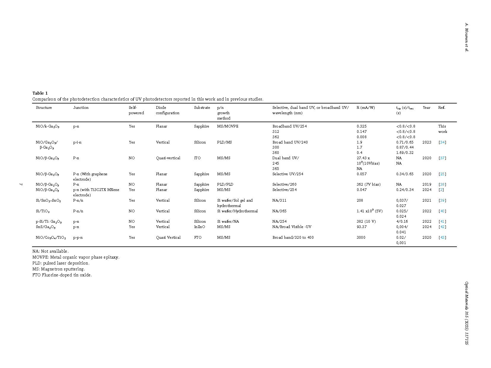
The bandgap width of a semiconductor is correlated with its light absorption properties, hence with the detection range. On the other hand, the different photodetector (PD) designs, such as planar or vertical, metal-semiconductor-metal (MSM) photoresistor, Schottky diodes (SBDs), p-n diodes (PNDs), p-i-n diodes (PINDs), leads to different photogeneration and carrier transport/collection mechanisms that control the device performance. Conventional silicon-based UV PDs have limitations due to the indirect and narrow bandgap of Si. In contrast, third-generation semiconductors, including wide-bandgap (WBG) materials, such as zinc oxide (ZnO), silicon carbide (SiC), gallium nitride (GaN), and their aluminum (Al)-alloy-based compounds, have demonstrated good photodetection capabilities. However, these materials exhibit significant limitations such as tendency to degradation of the epitaxial layers, particularly when the aluminum (Al) content is high. These limitations have triggered the development of ultrawide-bandgap (UWBG) semiconductors such as gallium oxide (Ga2O3), now widely studied in connection with fabrication of a new generation of solar-blind UVC detectors. On the other hand, a certain number of defects in Ga2O3, giving rise to appropriate energy states, may be advantageous as they enable sub-bandgap absorption, which contributes to extending detectivity towards the UVB band.
Abstract
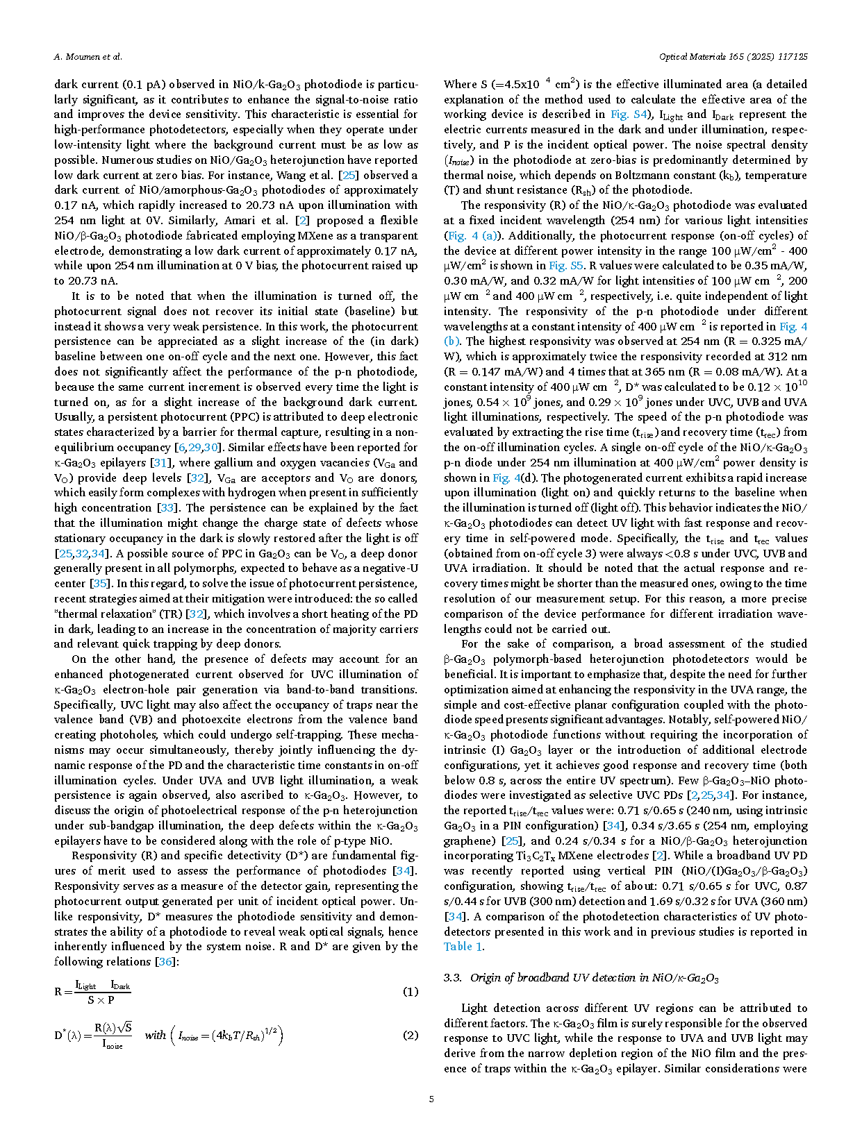
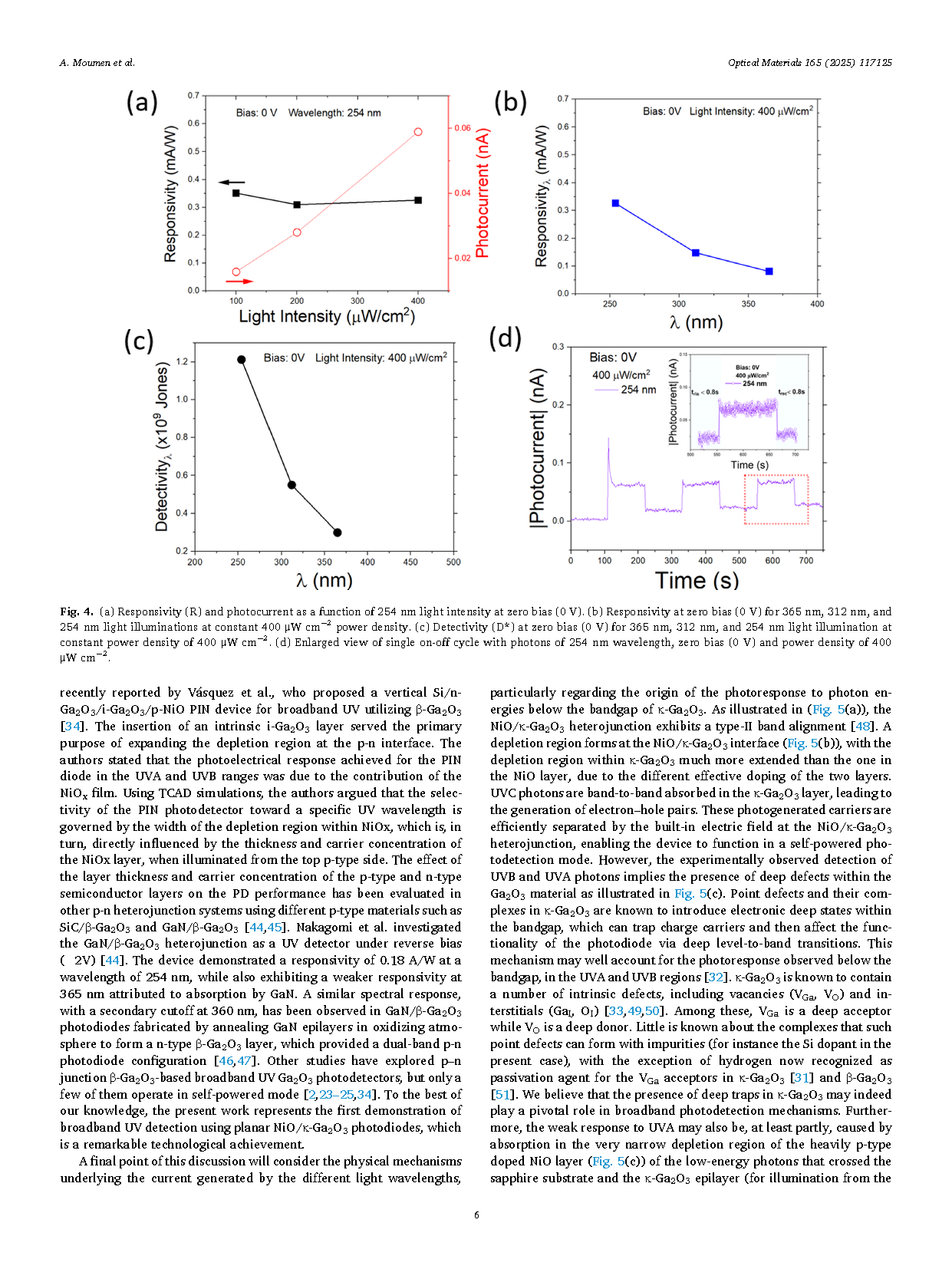
A novel broadband p-n UV photodiode is presented, that integrates an ultrawide band gap n-type κ-Ga2O3 epitaxial film doped with silicon (Si) and a p-type NiO polycrystalline film, to provide a planar NiO/κ-Ga2O3 p-n heterojunction for UV detection applications. The proposed device features a circular design, with a diameter of 240 μm, resulting in compactness and functionality, and represents the first demonstration of broadband UV detection using planar NiO/κ-Ga2O3 photodiodes. It can be operated in self-powered mode, which allows UV detection without use of an external power supply. The p-n photodiode exhibits excellent sensitivity to UVC light and acceptable sensitivity to UVB and UVA radiations. However, the response to UVA light is still weak and requires further optimization of the diode design. Response and recovery time below 0.8 s were observed for all UV illumination range. The presented photodiode has a simple design and shows significant potential in high-performance broadband UV detection in self-powered operation.
Conclusion
In conclusion, a self-powered broadband photodetector based on a NiO/κ-Ga2O3 p-n heterojunction was successfully fabricated and tested. The Si-doped κ-Ga2O3 epilayer was grown via MOVPE, while the polycrystalline NiO film was deposited using magnetron sputtering at RT. The diode was fabricated employing photolithography for precise patterning of circular planar geometry with a diameter of about 240 μm. The photodiode exhibited good rectifying behavior in dark conditions, and good responsivity and detectivity under UVC, UVB and UVA illumination. The UVC detection was particularly efficient while for other UV ranges the responsivity is lower. It is not yet understood what part of the UVB and UVA light is detected by the NiO depleted region and what is instead revealed thanks to photoionization of deep electronic states in the κ-Ga2O3 absorber. In all UV range, the photodiode showed fast photoresponse, with rise and recovery times of less than 0.8 s. In conclusion, this new device although conceptually simple showed potential for high-performance UV sensing applications.
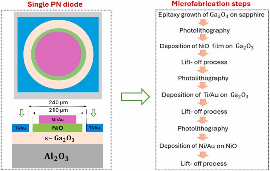
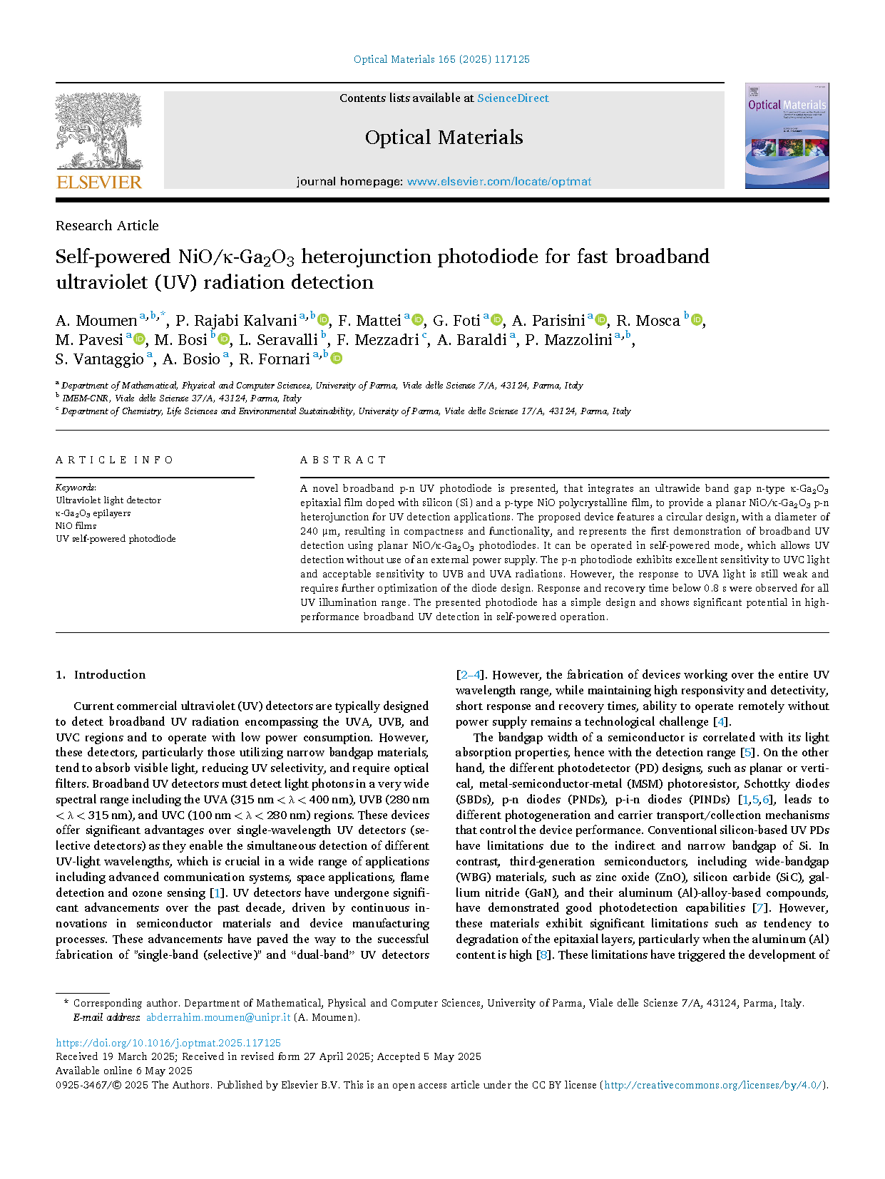
Fig. 1. Schematic of the NiO/Ga2O3 p−n photodiode with circular planar geometry, and description of the corresponding fabrication procedure.
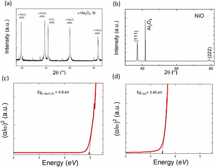
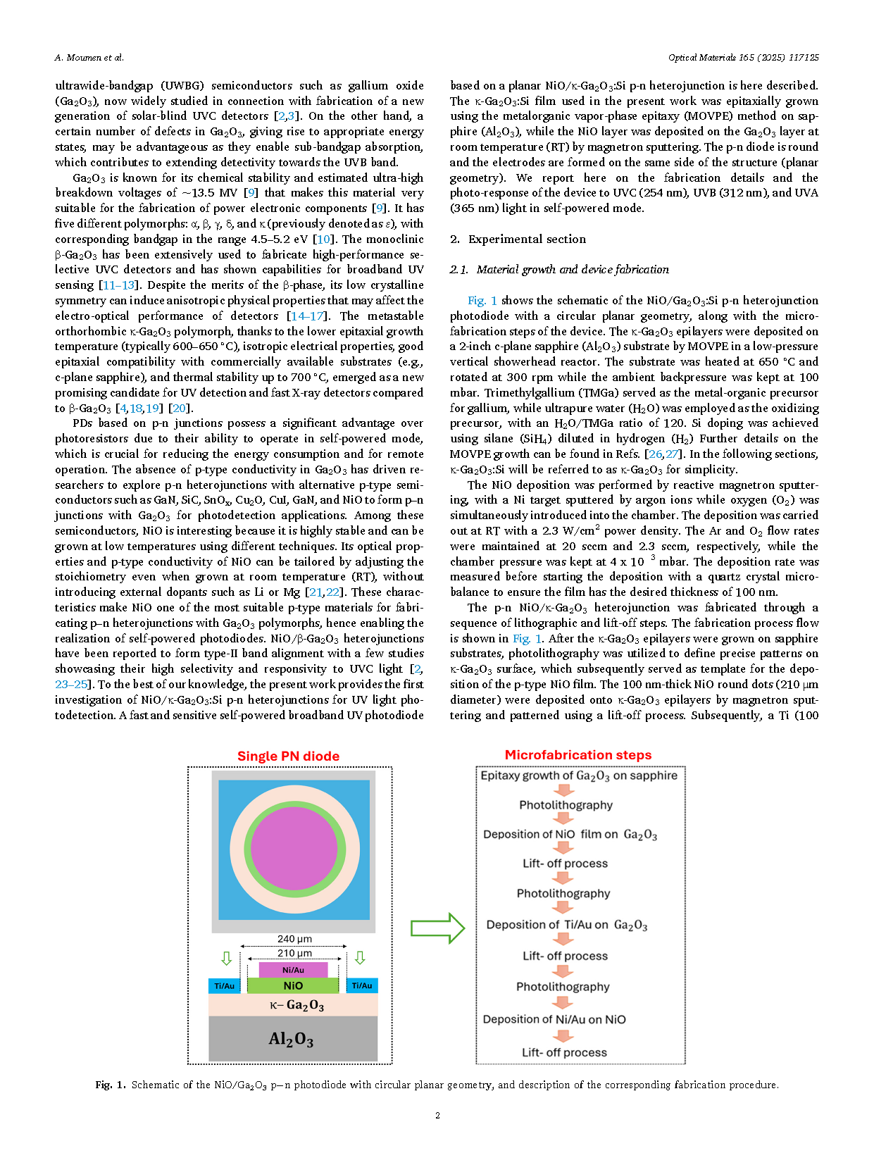
Fig. 2. (a) XRD patterns of κ-Ga2O3:Si epilayers. (b) XRD patterns of polycrystalline NiO film. (c) Tauc plot of κ-Ga2O3:Si epilayers. (d) Tauc plot of polycrystalline NiO film.
DOI:
doi.org/10.1016/j.optmat.2025.117125