Paper Sharing
【Domestic Papers】University of Science and Technology of China---Improved blocking capability of N-ion-implanted β-Ga₂O₃ U-shaped trench gate MOSFET by annealing in oxygen
日期:2025-05-27阅读:1012
Researchers from the University of Science and Technology of China have published a dissertation titled "Improved blocking capability of N-ion-implanted β-Ga2O3 U-shaped trench gate MOSFET by annealing in oxygen" in Applied Physics Express.
Project Support
This work was supported by the National Natural Science Foundation of China under Grant Nos. U23A20358, 62474170, 62404214 and 62234007, the National Key Research and Development Program of China under Grant No. 2024YFE0205200, the University of Science and Technology of China (USTC) Research Funds of the Double First-Class Initiative under Grant No. WK2100000055, the China Postdoctoral Science Foundation under Grant No. 2024M753114, the JieBang Headed Project of Changsha City Hunan Province under Grant No. kq2301006, and the Opening Project of and the Key Laboratory of Nanodevices and Applications in Suzhou Institute of Nano-Tech and Nano-Bionics of CAS. This work was partially carried out at the Center for Micro and Nanoscale Research and Fabrication, the Information Science Laboratory Center, the Instruments Center for Physical Science of USTC and the Nano Fabrication Facility of Suzhou Institute of Nano-Tech and Nano-Bionics, Chinese Academy of Sciences.
Background
β-Ga2O3 is a strong contender in next-generation high efficiency power conversion applications, considering its high critical electric field, which promises a lower specific on-resistance (Ron,sp) in unipolar devices than those based on SiC, GaN, etc., at the same voltage rating. In addition, high-quality large-diameter β-Ga2O3 substrates can be produced cost-effectively by various melt-growth methods.
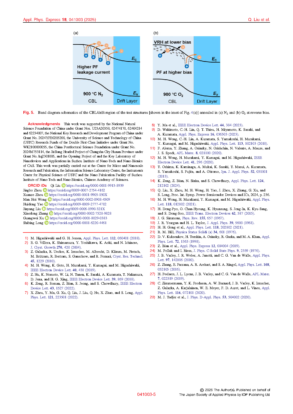
Vertical transistors are advantageous for high-power applications as they can reduce surface instabilities and enable voltage scaling without chip area expansion. As p-type doping is challenging in β-Ga2O3, currently enhancement-mode (E-mode) β-Ga2O3 vertical transistors can only be realized based on the accumulation channel or quasi-inversion channel formed at the surface of the current blocking layer (CBL). CBL in β-Ga2O3 is often formed by deep acceptor doping or by introducing compensating defects. However, vertical MOSFETs based on CBL usually suffer from a high leakage current and premature breakdown due to the limited voltage blocking capability of CBL. Lately, efforts have been made to optimize the voltage-sustaining capability of CBL. Mg-doped CBL achieves a Vbr over 1 kV through two-step annealing to dissociate Mg-H complexes in O2 ambient and increase Mg concentration. In N-ion-implanted CBL, the Vbr of U-shaped trench-gate MOSFET (UMOSFET) is improved to ∼1 kV by annealing at an elevated temperature. However, the Ron,sp of the device is significantly increased, possibly due to acceptor-like defect diffusion in the drift layer, suggesting that further optimization on activation annealing conditions is required.
Abstract
To improve the blocking capability of U-shaped trench gate MOSFETs (UMOSFETs) based on nitrogen-implanted current blocking layer (CBL), the post-implantation annealing atmosphere is optimized. Compared to the UMOSFET annealed in nitrogen, the oxygen-annealed device shows an improved breakdown voltage, increasing from 830 V to 1330 V, while maintaining similar specific on-resistance. By analyzing the leakage mechanisms of CBLs, the lower leakage current in the oxygen-annealed device is attributed to the reduced concentration of certain deep donors and the change in trap energy level involved in the Poole–Frenkel (PF) emission. This work validates oxygen annealing as an effective approach to optimizing nitrogen-implanted β-Ga2O3 power MOSFETs.
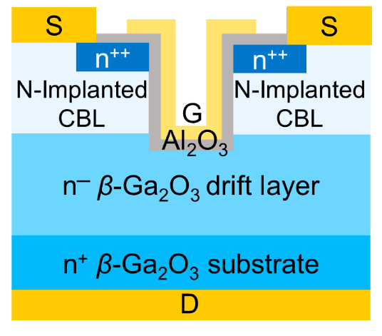
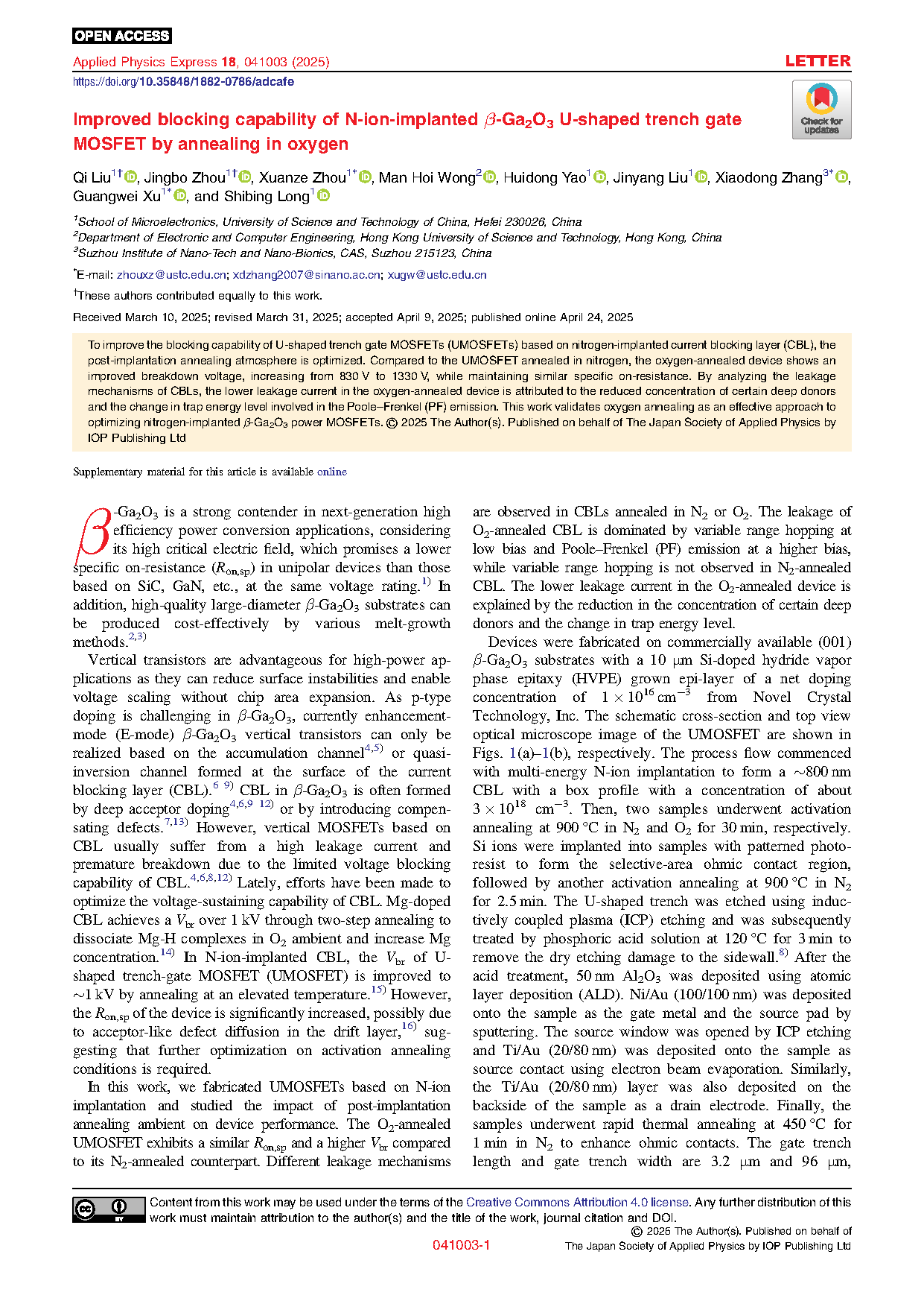
Fig. 1. Cross-sectional schematic diagram of the fabricated β-Ga2O3 UMOSFET.
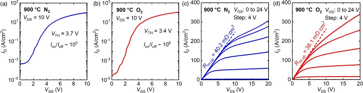
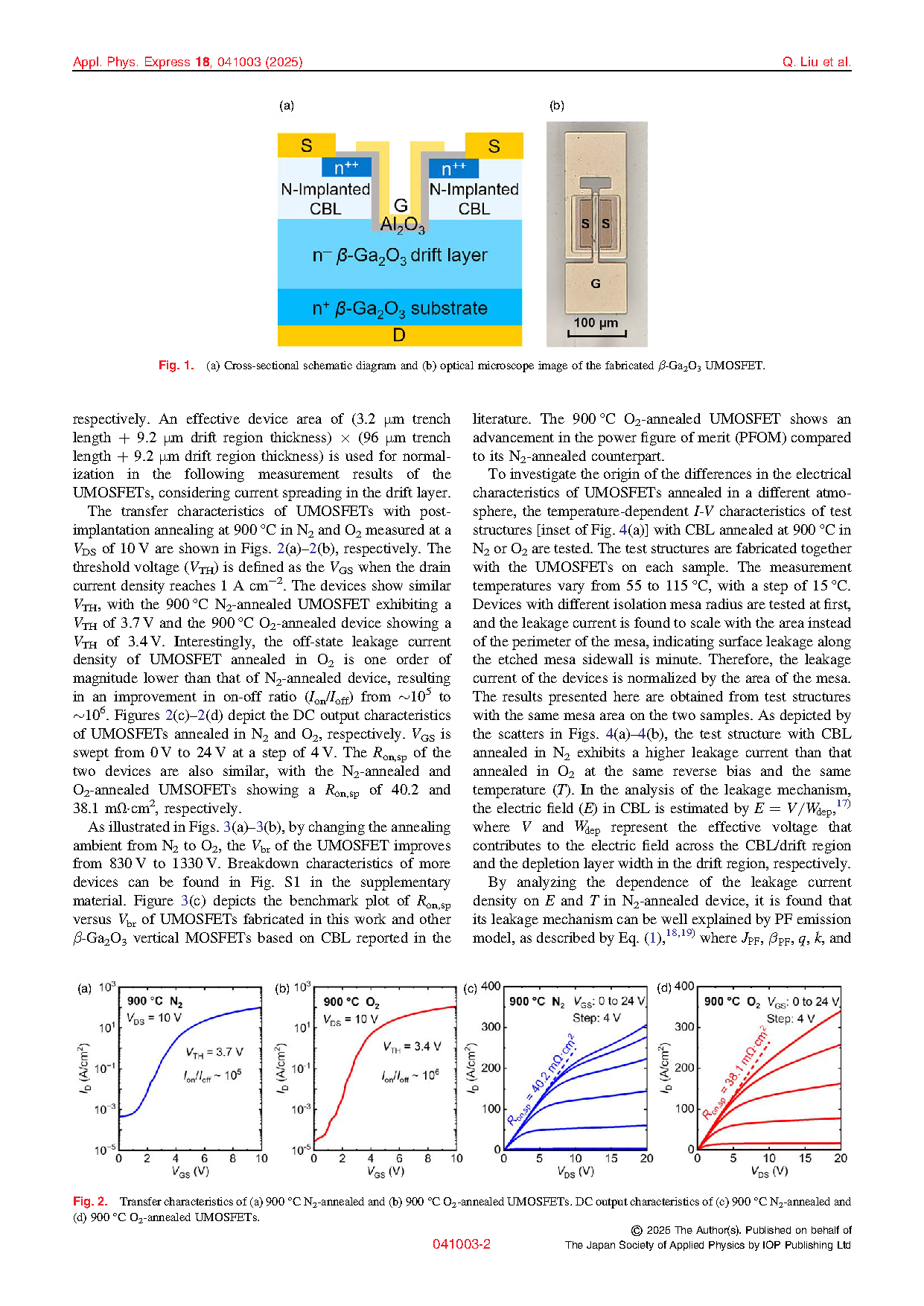
Fig. 2. Transfer characteristics of (a) 900 °C N2-annealed and (b) 900 °C O2-annealed UMOSFETs. DC output characteristics of (c) 900 °C N2-annealed and (d) 900 °C O2-annealed UMOSFETs.
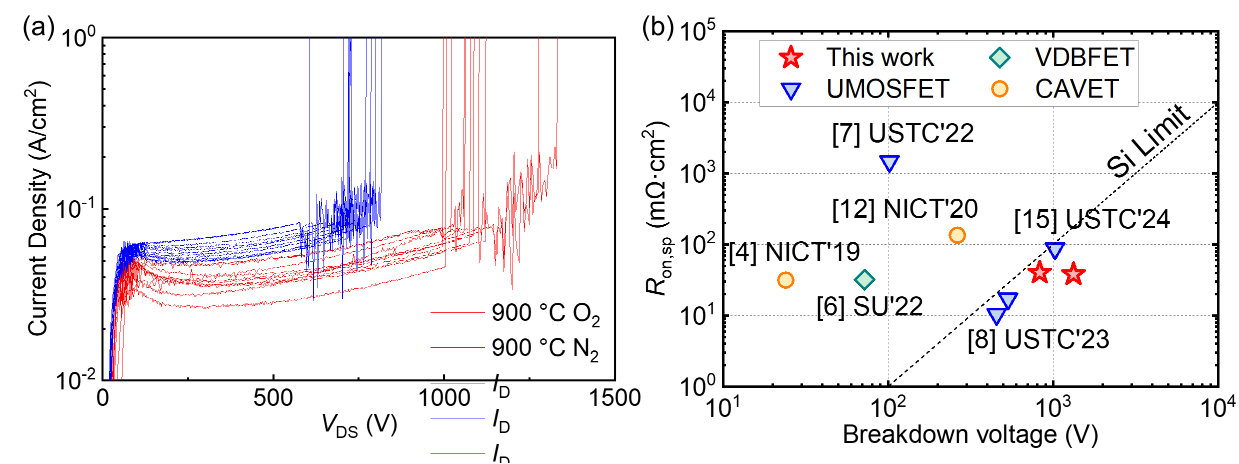
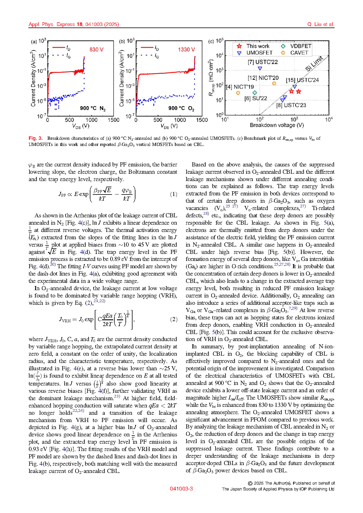
Fig. 3. (a) Breakdown characteristics of 900 ℃ N2-annealed (blue lines) and 900 ℃ O2-annealed (red lines) UMOSFETs. (b) Benchmark plot of Ron,sp versus Vbr of UMOSFETs in this work and other reported β-Ga2O3 vertical MOSFETs based on CBL.
DOI:
doi.org/10.35848/1882-0786/adcafe