Paper Sharing
【Member Papers】Xidian University---Interface modification-induced high-performance vertical NiOₓ/β-Ga₂O₃ heterojunction diodes via O₂ plasma treatment
日期:2025-05-23阅读:742
Researchers from the Xidian University have published a dissertation titled "Interface modification-induced high-performance vertical NiOx/β-Ga2O3 heterojunction diodes via O2 plasma treatment" in Applied Surface Science.
Project Support
This work was supported by the National Key R&D Program of China (No. 2022YFB3605402); the National Natural Science Foundation of China (under Grants 62274132, 62004151, 62274126).
Background
β-Gallium oxide (β-Ga2O3), as a potential material for the next generation of electronic devices due to its excellent material properties, elicits an incredible amount of interest. Moreover, large-sized, low-cost single-crystal substrates can be achieved through the melting or casting methods, which will facilitate the large-scale industrialization of Ga2O3 devices. Due to a lack of p-type Ga2O3, heterojunctions are the optimal solution to the technological bottleneck in the development of Ga2O3 devices. Recently, several groups have demonstrated various p-n heterojunction power diode (HJD) structures aimed at enhancing Ga2O3 device performance, including double-layered NiO, beveled-mesa, junction termination extension (JTE), field plate assisted deep mesa (FPDM). Concurrently, we have developed a composite terminal structure for NiO/β-Ga2O3 HJD with a power figure-of-merit of 13.2 GW/cm2 , that exceeds the 1-D unipolar limit of GaN and SiC. Notably, Jian-Sian Li et al. achieved breakdown voltages up to 13.5 kV and low on-resistance by optimizing the structure and process of NiO/β-Ga2O3 vertical heterojunction diodes, demonstrating their great potential for high power applications. In addition to developing advanced terminal structure designs, strengthening the research on the characteristics of heterojunction interfaces and transport mechanisms is crucial for improving the performance and accelerating industrialization of β-Ga2O3 heterojunction devices. Lu et al. achieved a performance-enhanced NiO/β-Ga2O3 HJD by obtaining high-quality heterojunction interfaces via TMAH treatment after ICP etching. Deng et al. investigated the interface energy band structure of NiO/β-Ga2O3 heterojunctions with different Ga2O3 orientations and its effect on the electrical properties. Wang et al. determined that bipolar charge transport in NiO/β-Ga2O3 HJD is dominated by the modified Shockley-Read-Hall recombination and minority carrier diffusion. Despite these advancements, research on the metal–semiconductor interface and optimization of ohmic contacts in NiOx/β-Ga2O3 HJDs remains largely unexplored.
Abstract
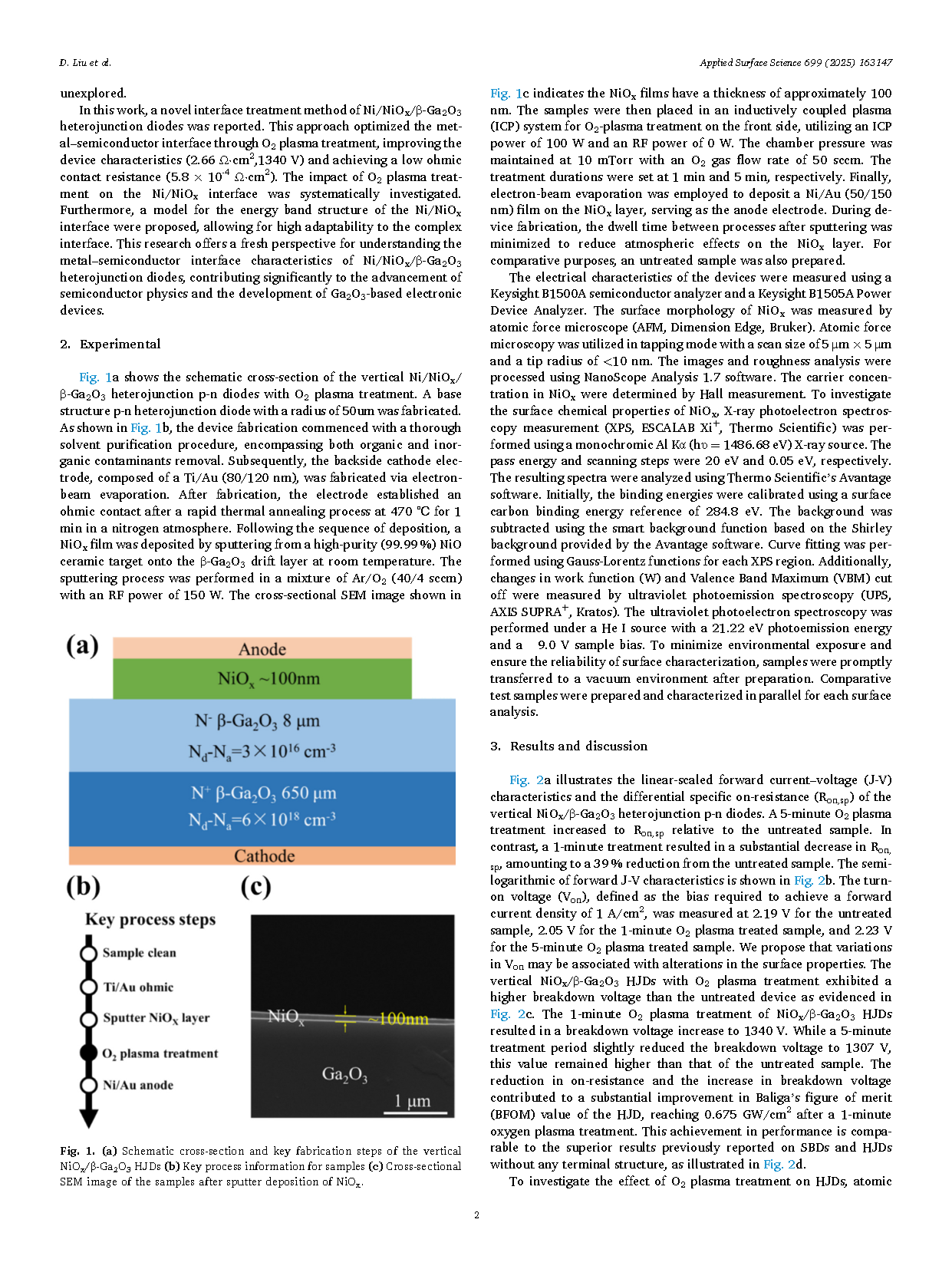
The advancement of NiOx/β-Ga2O3 heterojunctions is a crucial approach to overcoming the technical limitations of bipolar Ga2O3 power devices. However, the development of interface engineering and the investigation of ohmic characteristics at the metal-NiOx interface remain largely unexplored. In this study, we demonstrated that O2 plasma treatment at a specific time can achieve low ohmic contact resistance (5.8 × 10⁻⁴ Ω·cm2) and high breakdown voltage (1340 V) for Ni/NiOx/β-Ga2O3 heterojunction diodes, which outperforms most of state-of-the-art Ga2O3 heterojunction diodes and Schottky barrier diodes without any terminal structures. The comparative analysis revealed that the variations of NiOOH content at the interface play a pivotal role in affecting the interface properties and the device’s forward characteristics. Following O2 plasma treatment at a specific duration, the increased presence of the strong dipole NiOOH altered the Ni/NiOx interface state, leading to a significant increase in hole concentration on the NiOx surface, enhanced transport ability of interface carriers, and a substantial reduction in ohmic contact resistance. This study bridges the knowledge gap between the characteristics of metal–semiconductor interfaces and the ohmic transport mechanism in β-Ga2O3 heterojunctions, offering significant insights for the design and optimization of β-Ga2O3 heterojunction devices.
Highlights
• O2 plasma treatment achieves low ohmic resistance and high breakdown voltage in NiOx/β-Ga2O3
• Variations in NiOOH content at the interface affect the interface properties and device’s forward characteristics.
• Specific O2 plasma treatment duration modifies Ni/NiOx interface, enhancing ohmic contact properties.
Conclusions
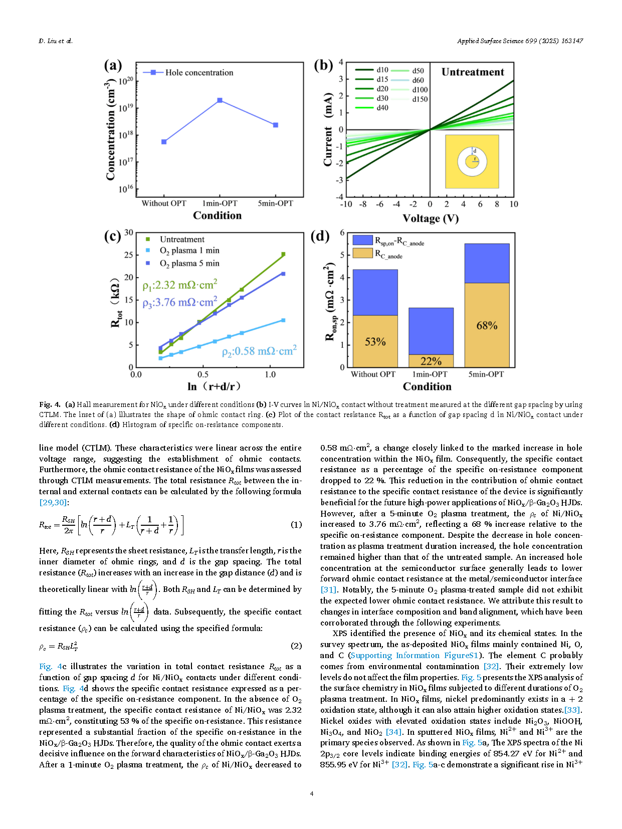
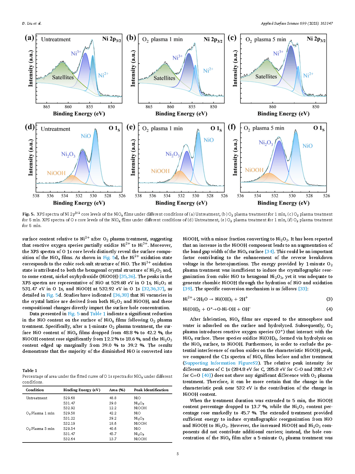
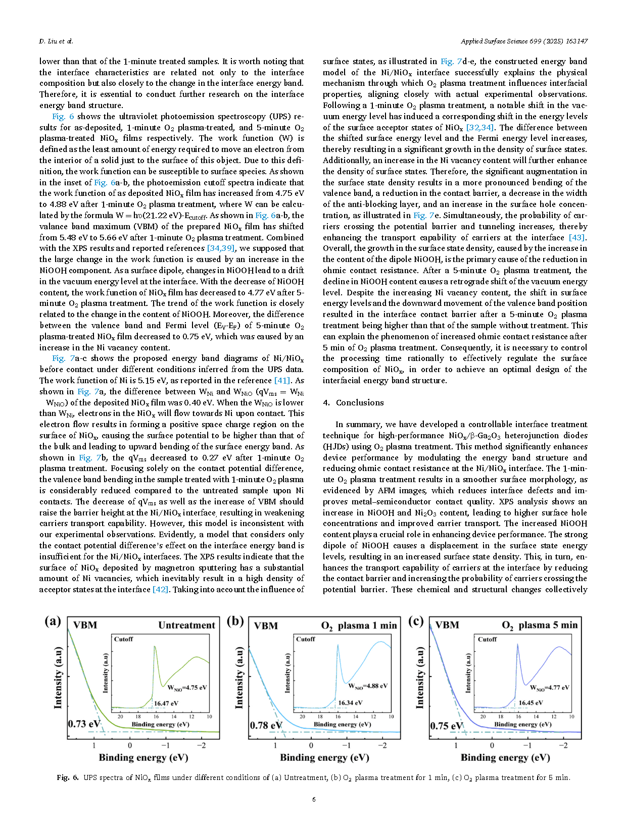
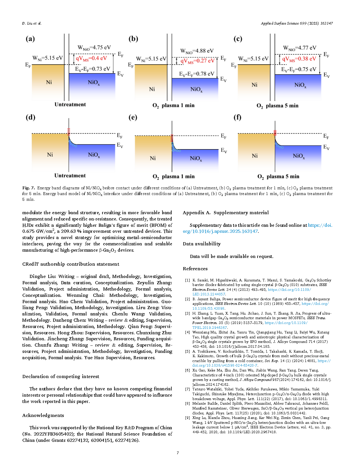
In summary, we have developed a controllable interface treatment technique for high-performance NiOx/β-Ga2O3 heterojunction diodes (HJDs) using O2 plasma treatment. This method significantly enhances device performance by modulating the energy band structure and reducing ohmic contact resistance at the Ni/NiOx interface. The 1-minute O2 plasma treatment results in a smoother surface morphology, as evidenced by AFM images, which reduces interface defects and improves metal–semiconductor contact quality. XPS analysis shows an increase in NiOOH and Ni2O3 content, leading to higher surface hole concentrations and improved carrier transport. The increased NiOOH content plays a crucial role in enhancing device performance. The strong dipole of NiOOH causes a displacement in the surface state energy levels, resulting in an increased surface state density. This, in turn, enhances the transport capability of carriers at the interface by reducing the contact barrier and increasing the probability of carriers crossing the potential barrier. These chemical and structural changes collectively modulate the energy band structure, resulting in more favorable band alignment and reduced specific on-resistance. Consequently, the treated HJDs exhibit a significantly higher Baliga’s figure of merit (BFOM) of 0.675 GW/cm2, a 209.63 % improvement over untreated devices. This study provides a novel strategy for optimizing metal–semiconductor interfaces, paving the way for the commercialization and scalable manufacturing of high-performance β-Ga2O3 devices.
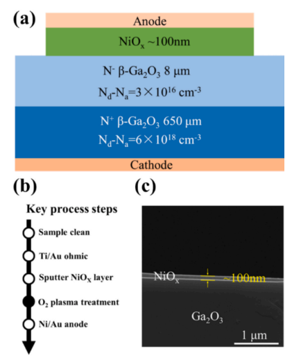
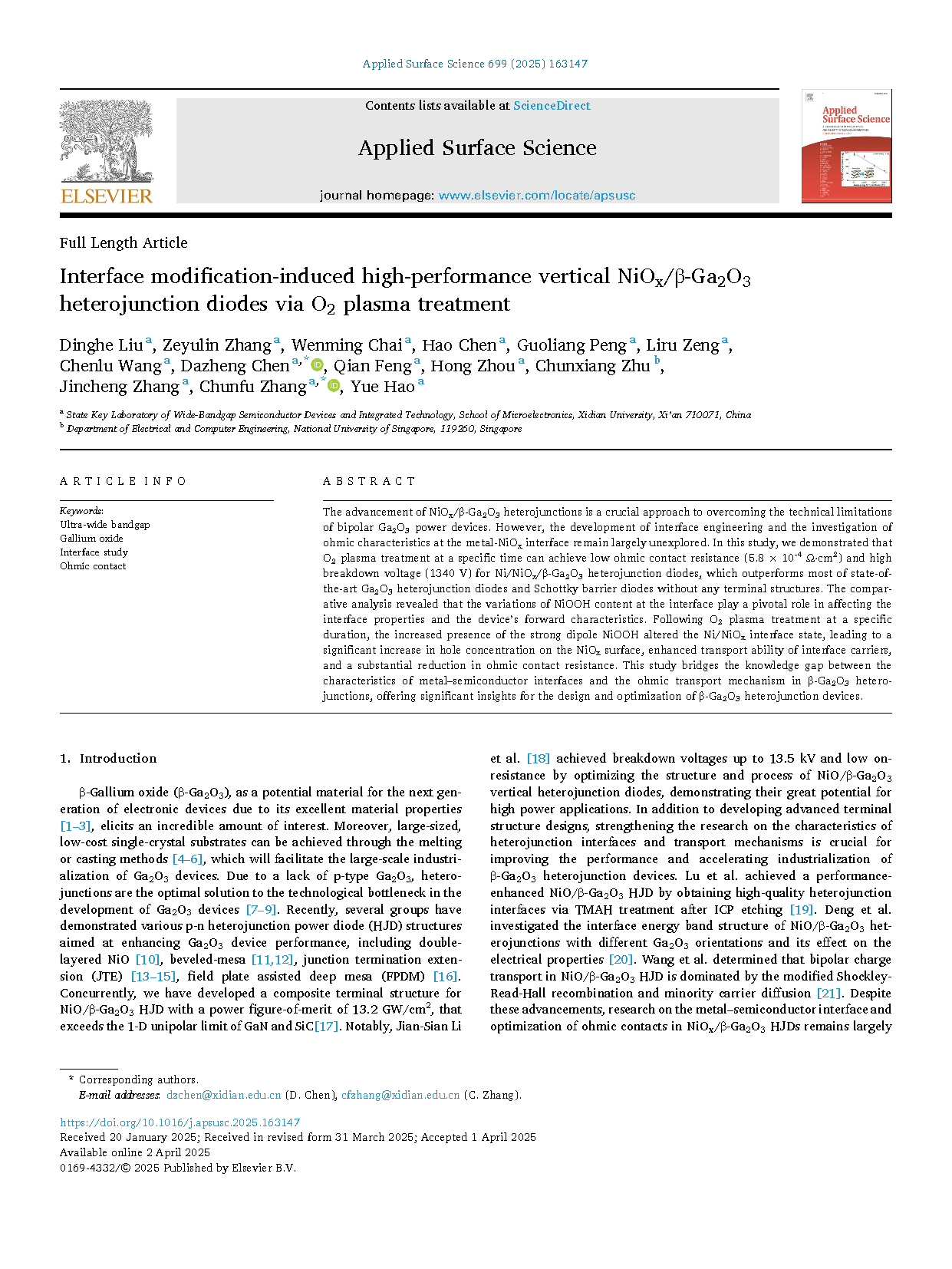
Fig. 1. (a) Schematic cross-section and key fabrication steps of the vertical NiOx/β-Ga2O3 HJDs (b) Key process information for samples (c) Cross-sectional SEM image of the samples after sputter deposition of NiOx.
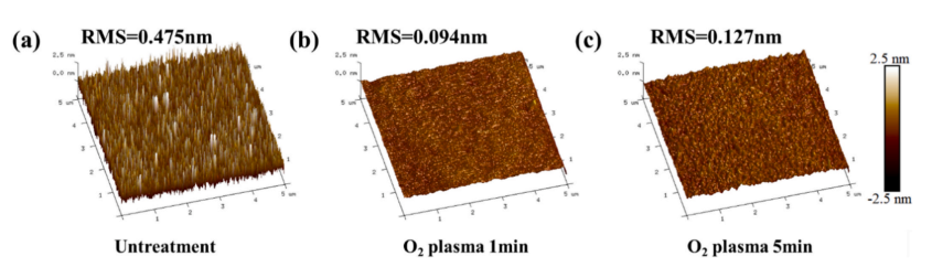
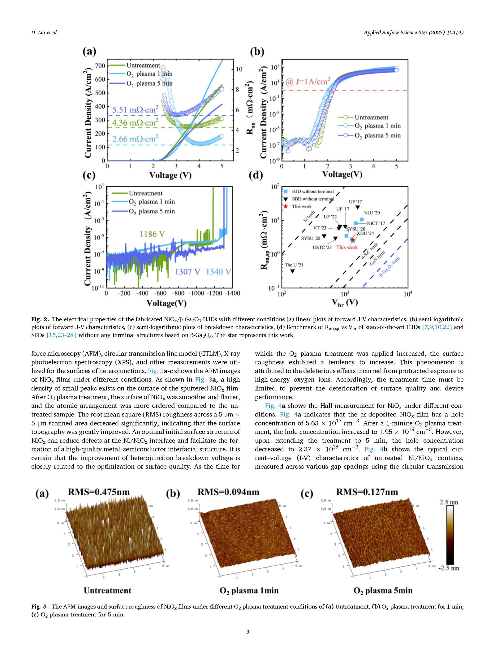
Fig. 2. The AFM images and surface roughness of NiOx films under different O2 plasma treatment conditions of (a) Untreatment, (b) O2 plasma treatment for 1 min, (c) O2 plasma treatment for 5 min.
DOI:
doi.org/10.1016/j.apsusc.2025.163147