Paper Sharing
【Member Papers】Nanjing University---Boosting photoelectrochemical performance on α-Ga₂O₃ nanowire arrays by indium cation doping for self-powered ultraviolet detection
日期:2025-05-14阅读:728
Researchers from the Nanjing University of Posts and Telecommunications have published a dissertation titled "Boosting photoelectrochemical performance on α-Ga2O3 nanowire arrays by indium cation doping for self-powered ultraviolet detection" in Journal of Semiconductors.
Project support
This work was supported by the National Key Research and Development Program of China (2023YFB3610500); National Natural Science Foundation of China (62104110, 62374094); the Project funded by China Postdoctoral Science Foundation (2023T160332), and Natural Science Foundation of Nanjing University of Posts and Telecommunications (NY224084, NY224131).
Background
Extensive investigations have been conducted on ultraviolet (UV) detectors because of their broad applications in environmental monitoring, gas sensing, medical diagnostics, and military early warning systems. Among ultraviolet detectors, solid-state UV detectors require complex fabrication processes and additional driving voltages for operation, and their relatively slow response times severely limit their practical applications. Photoelectrochemical (PEC) UV detectors, on the other hand, are attracting growing interest as photovoltaic devices owing to their low cost, simplicity in fabrication, and remarkable self-powering capabilities. In addition to the physical processes of charge carrier separation and transport, PEC UV detectors are also associated with interfacial chemical reactions, where different electrolytes offer more avenues for performance modulation. Therefore, PEC UV detectors are especially fitting for underwater optoelectronic equipment.
Abstract
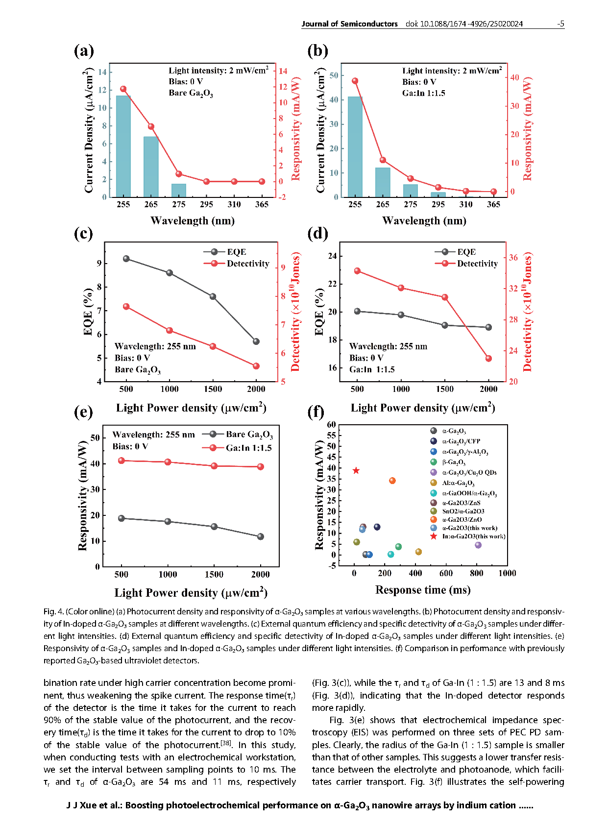
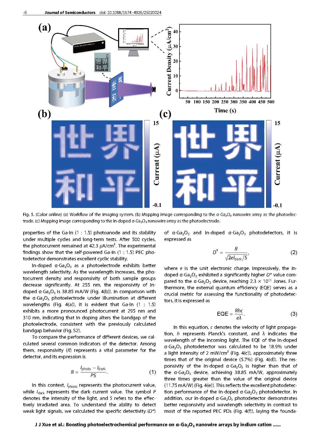
Low power consumption, high responsivity, and self-powering are key objectives for photoelectrochemical ultraviolet detectors. In this research, In-doped α-Ga₂O₃ nanowire arrays were fabricated on FTO substrates through a hydrothermal approach, with subsequent thermal annealing. These arrays were then used as photoanodes to construct a UV photodetector. In doping reduced the bandgap of α-Ga₂O₃, enhancing its absorption of UV light. Consequently, the In-doped α-Ga₂O₃ nanowire arrays exhibited excellent light detection performance. When irradiated by 255 nm deep ultraviolet light, they obtained a responsivity of 38.85 mA/W. Moreover, the detector's response and recovery times are 13 and 8 ms respectively. The In-doped α-Ga₂O₃ nanowire arrays exhibit a responsivity that is about three-fold higher than the undoped one. Due to its superior responsivity, the In-doped device was used to develop a photoelectric imaging system. This study demonstrates that doping α-Ga₂O₃ nanowires with indium is a potent approach for optimizing their photoelectrochemical performance, which also has significant potential for optoelectronic applications.
Conclusion
In summary, we fabricated indium-doped α-Ga₂O₃ nanowire arrays on FTO substrates through a straightforward, cost-effective hydrothermal process, followed by annealing. These nanowire arrays were then employed to fabricate a self-powered photoelectrochemical UV detector. The results of verification suggest that the In-doped α-Ga₂O₃ nanowire arrays grown on the FTO substrate exhibit excellent photodetection capabilities. with a peak responsivity of approximately 38.85 mA/W. In contrast with the undoped device, the indium-doped device exhibited approximately three times higher peak responsivity and a faster response speed. Furthermore, the remarkable performance of this self-powered UV detector enabled the development of a photoelectric imaging system. This study reveals that incorporating indium is a potent approach to modulating the photoelectrochemical performance of α-Ga₂O₃ nanowires, highlighting significant application potential for indium-doped α-Ga₂O₃ nanowire arrays in optoelectronic devices.
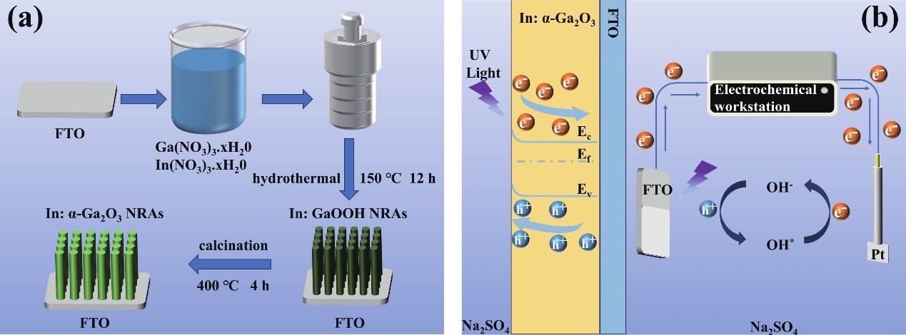
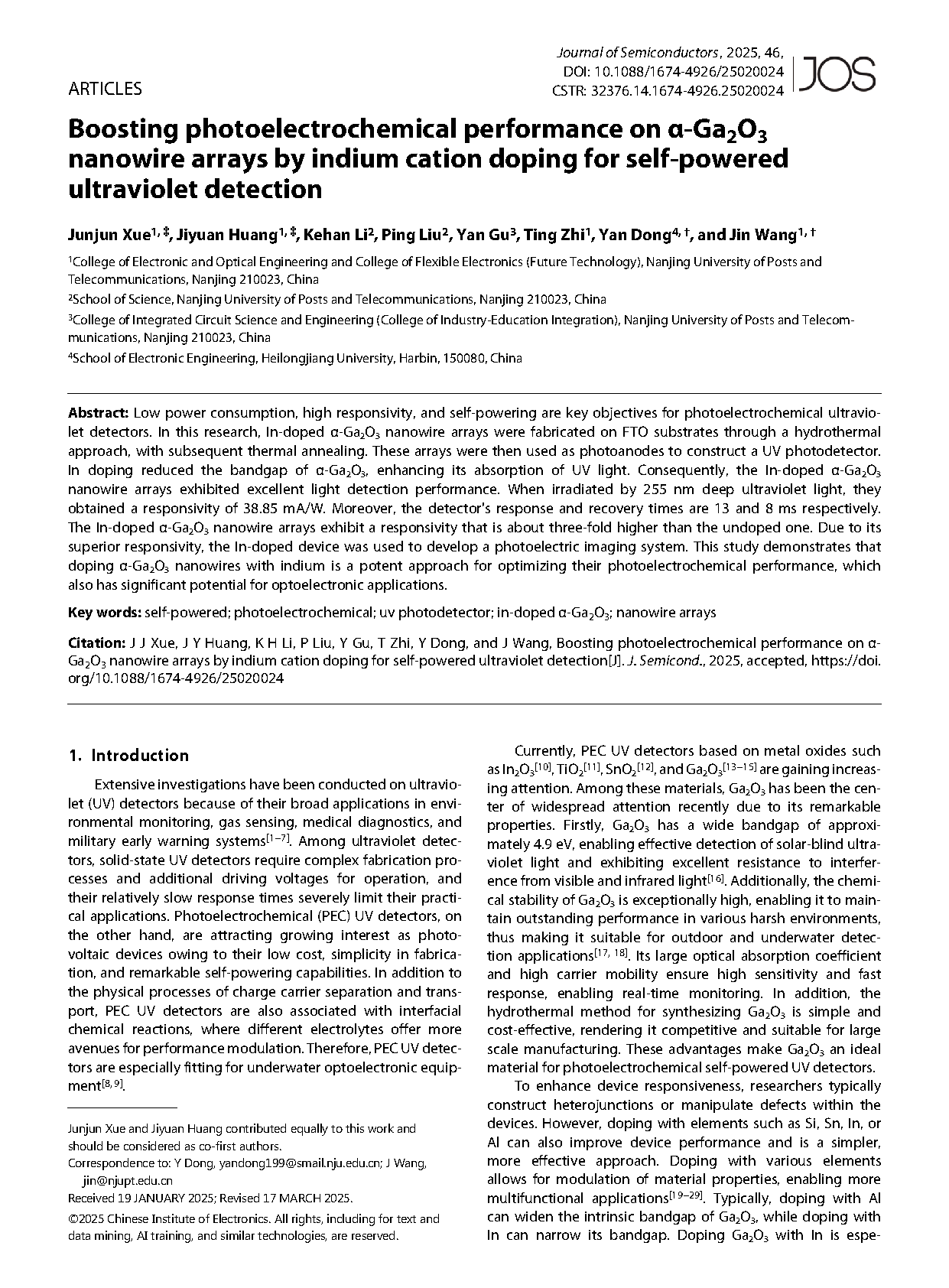
Fig. 1. (a) Schematic diagram of the preparation process for In-doped α-Ga₂O₃ nanowire arrays. (b) Illustration of the photoelectrochemical working mechanism of the In-doped α-Ga₂O₃ photoanode.
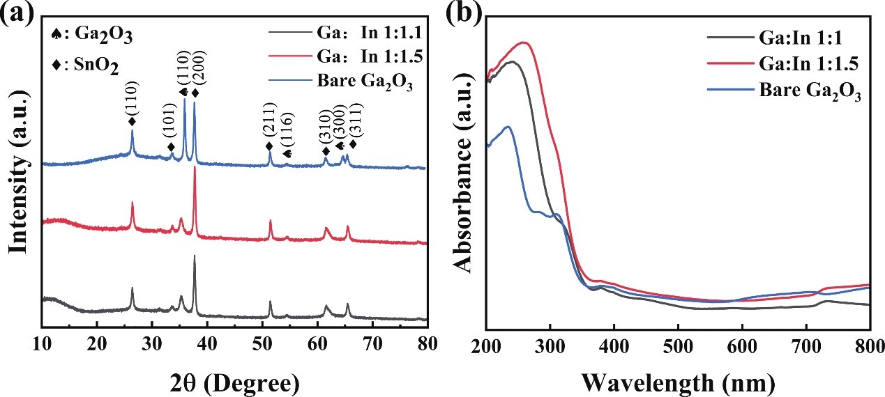
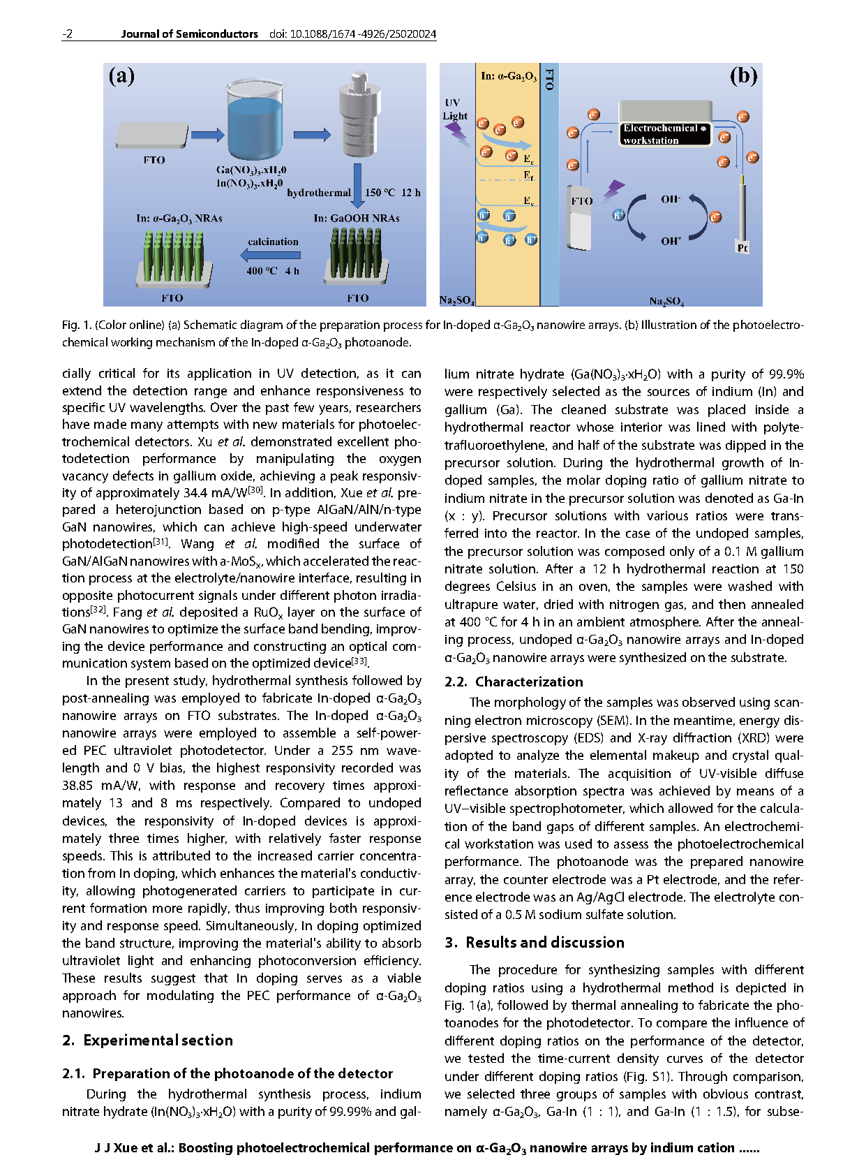
Fig. 2. (a) X-ray diffraction (XRD) patterns of indium-doped α-Ga₂O₃ samples. (b) UV−Visible absorption spectra of indium-doped α-Ga₂O₃ samples.
DOI:
doi.org/10.1088/1674-4926/25020024