Paper Sharing
【International Papers】Trap states and hydrogenation of implanted Si in semi-insulating Ga₂O₃(Fe)
日期:2025-05-13阅读:571
Researchers from the National University of Science and Technology MISiS have published a dissertation titled " Trap states and hydrogenation of implanted Si in semi-insulating Ga2O3(Fe)" in Journal of Vacuum Science & Technology A.
Project Support
The work at NUST MISIS was supported in part by a grant from the Ministry of Science and Higher Education of Russian Federation (Agreement No. 075-15-2022-1113). The work at UF was performed as part of Interaction of Ionizing Radiation with Matter University Research Alliance (IIRM-URA), sponsored by the Department of the Defense, Defense Threat Reduction Agency, under Award No. HDTRA1-20-2-0002.
Background
β-Ga2O3, with its ultra-wide bandgap (~4.8 eV) and high breakdown field (8–10 MV/cm), is a promising material for next-generation high-power electronics and UV photodetectors. One key challenge in device fabrication is controlled doping, which is crucial for tailoring electrical properties. Si ion implantation is commonly used to introduce n-type doping into β-Ga2O3, but the process often leads to unintended defect formation and carrier compensation, reducing activation efficiency.
Additionally, hydrogen passivation is known to affect defect states and doping behavior in semiconductors. While hydrogenation has been shown to improve electrical performance in some materials, its effects on Si-implanted β-Ga2O3 remain poorly understood. This study investigates the electrical properties, deep trap states, and hydrogenation effects in Si-implanted semi-insulating Fe-doped β-Ga2O3.
Abstract
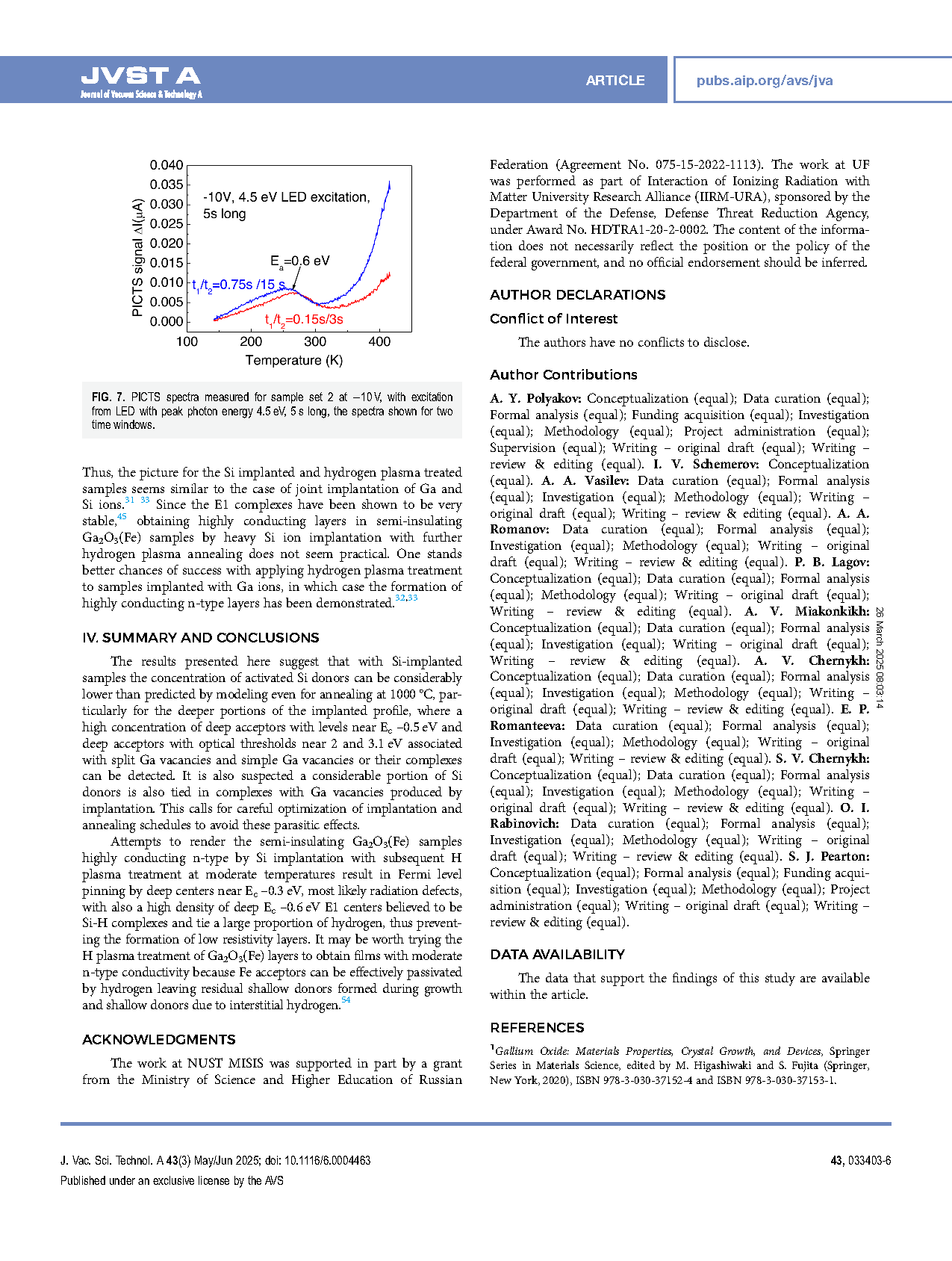
The electrical properties and deep trap spectra of semi-insulating Ga2O3(Fe) implanted with Si ions and subsequently annealed at 1000 °C were investigated. A significant discrepancy was observed between the measured shallow donor concentration profile and the profile predicted by Stopping Power and Range of Ions in Matter simulations, indicating substantial compensation. Deep level transient spectroscopy revealed the presence of deep acceptors at Ec −0.5 eV with a concentration of ∼10¹⁷ cm−³, insufficient to fully account for the observed compensation. Photocapacitance spectroscopy identified additional deep acceptors with optical ionization thresholds near 2 and 2.8–3.1 eV, tentatively attributed to gallium vacancy-related defects. However, the combined concentration of these deep acceptors still fell short of explaining the observed donor deactivation, suggesting the formation of electrically neutral Si-vacancy complexes. Furthermore, the properties of Ga2O3 (Fe) implanted with Si and subjected to hydrogen plasma treatment at 330 °C were also examined. This material exhibited high resistivity with the Fermi level pinned near Ec –0.3 eV, similar to common radiation defects in proton-implanted Ga2O3. A prominent deep center near Ec −0.6 eV, consistent with the known E1 electron trap attributed to Si-H complexes, was also observed. These results highlight the challenges associated with Si implantation and activation in Ga2O3 and suggest that hydrogen plasma treatment, while effective for Ga-implanted Ga2O3 is less suitable for Si-implanted material due to the formation of compensating Si-H complexes.

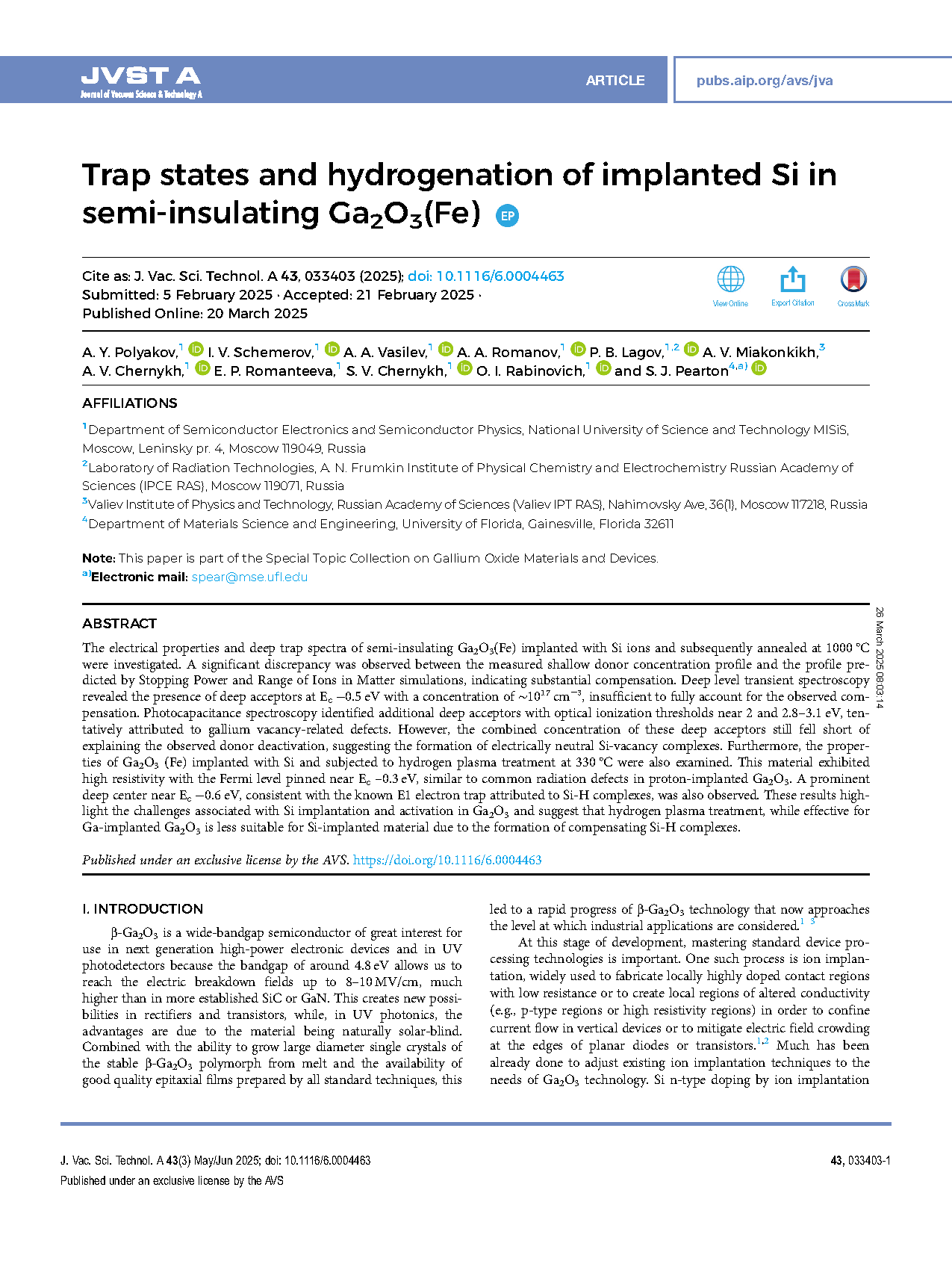
FIG. 1. Expected distribution of implanted Si based on SRIM modeling.
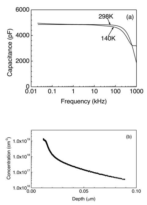
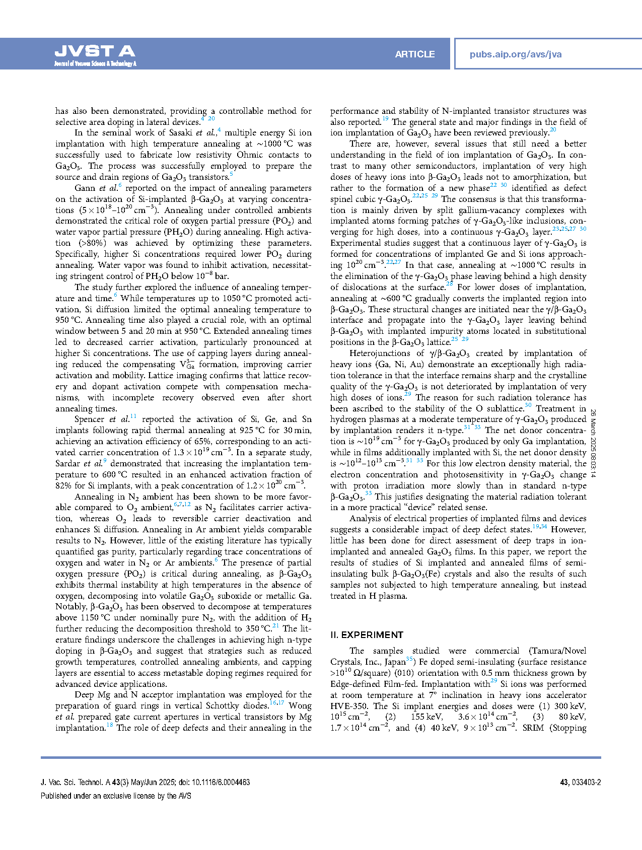
FIG. 2. (a) C–f characteristics of the implanted and annealed sample set 1 measured at 0 V and 100 kHz at 298 and 140 K; (b) the depth profile of electron concentration at room temperature calculated from C–V characteristic measured at 100 kHz.
DOI:
doi.org/10.1116/6.0004463