


论文分享
【会员论文】南京邮电大学唐为华等:锡掺杂诱导氧化镓深紫外光电探测器界面势垒高度裁剪
日期:2025-09-23阅读:470
本文要点
这项研究强调了平衡掺杂浓度与性能优化的重要性,揭示了界面工程对半导体器件电子传输行为及性能调控的重要潜力。
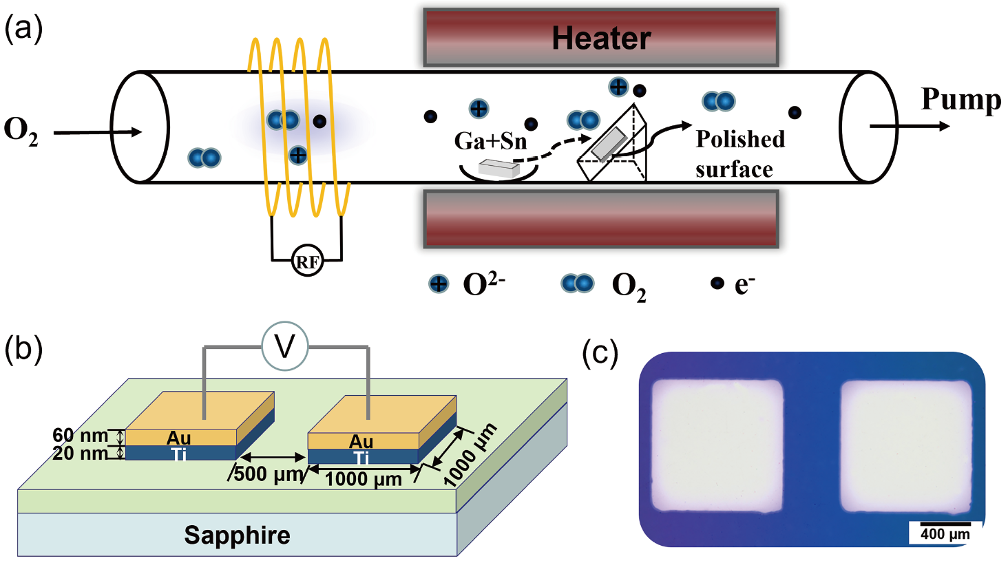
Figure 1. (a) Schematic diagram of the PECVD system. (b) Structure diagram and (c) top-view microscopy image of the fabricated Sn-doped Ga2O3 film-based PD.
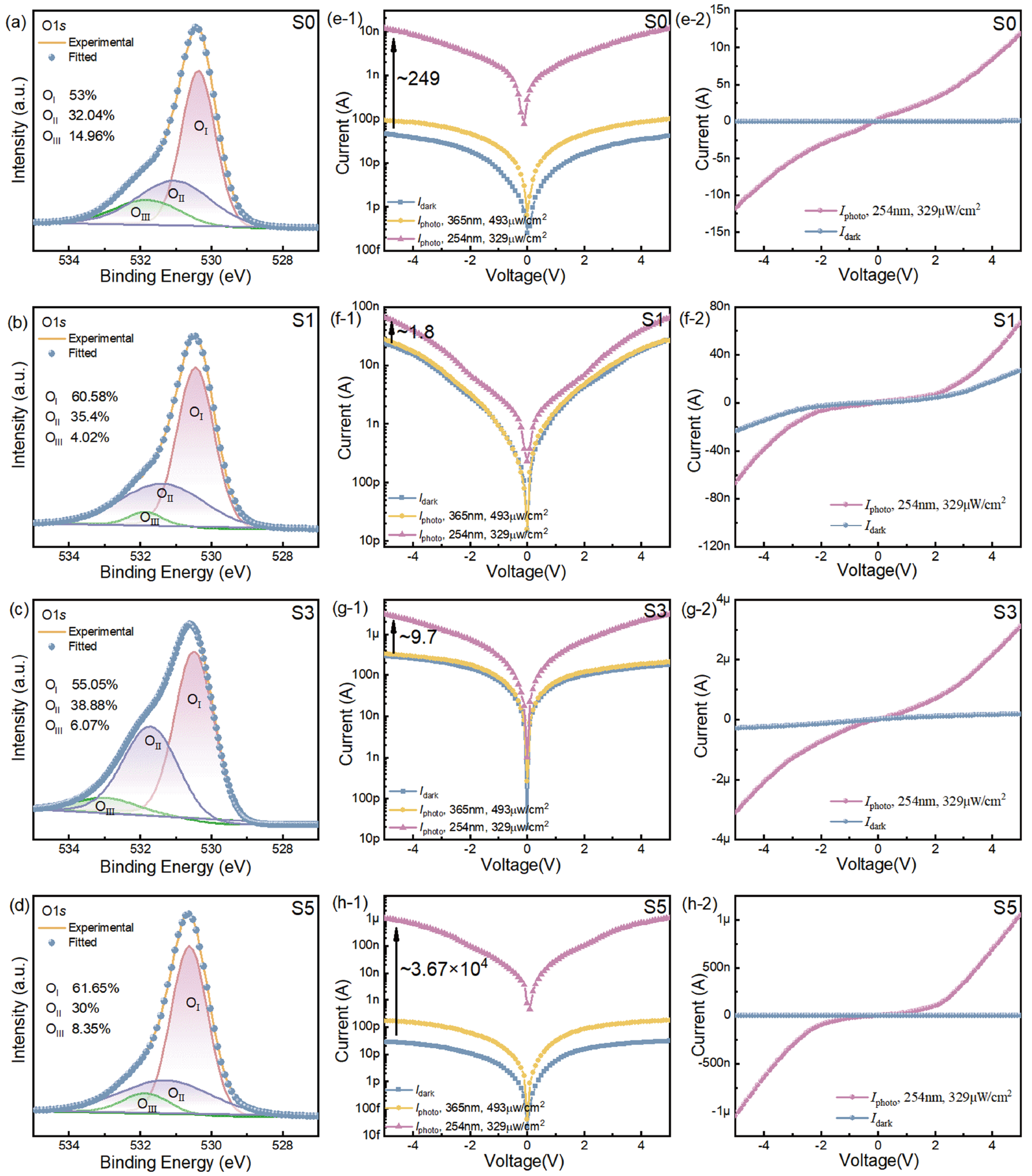
Figure 2. O 1s high-resolution XPS spectra of (a) S0, (b) S1, (c) S3, and (d) S5 samples. The log-scale (1) and linear (2) I-V characteristics of the corresponding (e) S0, (f) S1, (g) S3, and (h) S5 devices under dark conditions and light illumination.
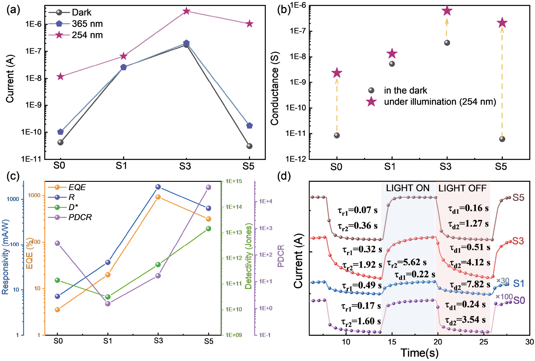
Figure 3. (a) Current and (b) conductance comparison of S0–S5 devices under dark conditions and light illumination. (c) EQE, R, D*, and PDCR comparison of S0–S5 devices. (d) I-t curves of S0–S5 devices.
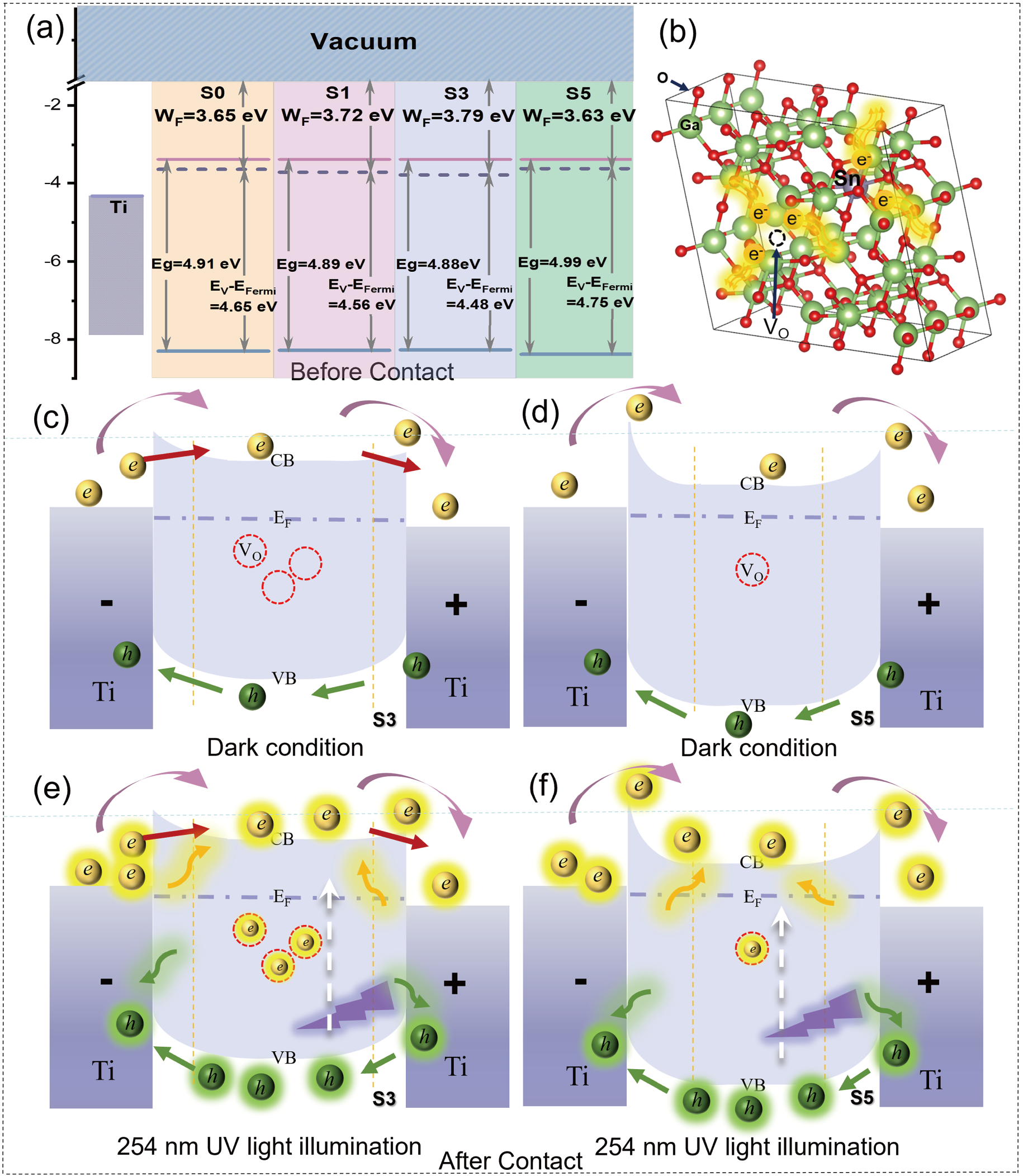
Figure 4. (a) Schematic diagram of energy band structural evolution of S0–S5 samples before contacting with the Ti electrode. (b) Strategy of donor doping to improve conductivity. Operating mechanism of the S3 and S5 devices (c, d) under the dark condition, and (e, f) under UV light illumination with bias after contacting with Ti electrodes.
DOI:
https://doi.org/10.1007/s40843-025-3509-0
