


Discover
【Knowledge Discover】Panoramic Review of Gallium Oxide (Issue 4) | How Far Is Gallium Oxide from “Super Power Devices”?
日期:2026-06-05阅读:61
Introduction:
In the first three issues, we explored gallium oxide (Gallium Oxide) from the perspectives of its material value, crystal structure, and key physical parameters, gradually uncovering the unique advantages of this ultra-wide bandgap semiconductor. Gallium oxide has attracted widespread attention precisely because its bandgap width, critical breakdown field, and theoretical performance in power devices demonstrate a unique potential beyond conventional wide-bandgap semiconductors, promising to break through the performance limits of existing power devices and achieve “superior performance.” But as these impressive material parameters move toward real devices and industrial applications, how far is gallium oxide from becoming a “super power device”?
With an ultra-wide bandgap of up to 4.9 eV and an extremely high critical breakdown field of about 8 MV/cm, the theoretical potential of gallium oxide is already evident. However, moving from laboratory research to mature commercial applications, any new semiconductor material must undergo rigorous engineering challenges: How can the p-type doping issue be overcome? How can fragile dielectric layers be effectively protected under ultra-high electric fields? And how can the heat dissipation bottleneck caused by its intrinsically low thermal conductivity be resolved?
This issue approaches gallium oxide from the perspective of industrial application, combining insights from large-size melt-grown crystals, heterojunction band engineering, dielectric reliability under extreme electric fields, and system-level thermal management, to map out the hardcore path for gallium oxide to move from its theoretical limits toward industrial-scale production.
Issue 4
How Far Is Gallium Oxide from Becoming a “Super Power Device”?
Foundational Support:
Industrial Breakthrough in Large-Scale Melt-Growth Crystals
The commercial adoption of any power device relies fundamentally on low-cost, high-quality, and scalable substrate materials.
Unlike the relatively slow and costly vapor-phase growth process of 4H-SiC, β-Gallium Oxide is currently one of the few ultra-wide bandgap semiconductor materials that can grow large single crystals via atmospheric-pressure melt growth. This characteristic provides gallium oxide with a high growth rate and excellent diameter-expansion potential, forming a crucial foundational advantage for its path toward industrialization.
However, large size does not inherently mean high quality. For Gallium Oxide substrates, key factors determining industrial competitiveness include reducing thermal stress and controlling dislocation density during crystal growth, as well as achieving high surface flatness and low-damage cutting, grinding, and polishing during subsequent processing.
On this critical track, the Gallium Oxide industry continues to refine its capabilities across crystal growth, wafer processing, epitaxial preparation, device development, and core equipment—both in international industrial layouts and domestic technological advancement. Currently, the industry has made significant progress in the large-scale production of 2–4 inch single-crystal substrates, the development of large melt-growth crystal equipment, and subsequent epitaxial and device verification. From foundational substrate materials to key equipment, and then to epitaxial and device applications, this gradual integration is helping Gallium Oxide move from theoretical material potential toward a clearer path to industrialization.
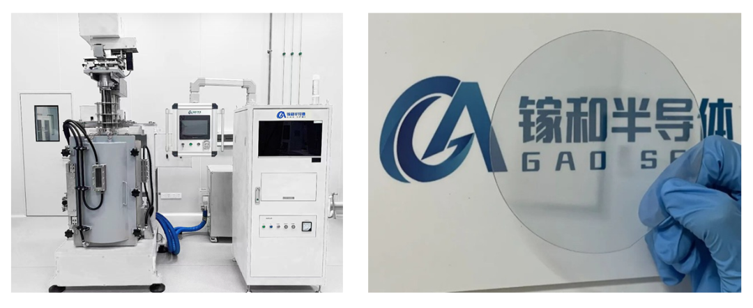
(Left) Large-scale Gallium Oxide single-crystal growth furnace developed independently by Ga & Semiconductor;
(Right) High-quality large Gallium Oxide single-crystal substrates produced at scale using core equipment.)
Breaking the Physical Bottleneck:
Heterostructure Design to Circumvent p-Type Doping Limitations
While the breakthrough in large-size substrates demonstrates Gallium Oxide’s advantages in material preparation and scalable supply, p-type doping remains a fundamental physical challenge in power device design. In traditional silicon- or SiC-based power devices, high-quality p–n junctions are essential for achieving high breakdown voltage, low leakage current, and avalanche energy tolerance.
However, for β-Gallium Oxide, the valence band maximum is relatively flat, resulting in a large hole effective mass, which makes holes prone to self-trapping within the lattice. Additionally, acceptor impurities typically have high activation energies and may exhibit significant self-compensation effects, making stable, high-conductivity p-type doping in Gallium Oxide extremely challenging.
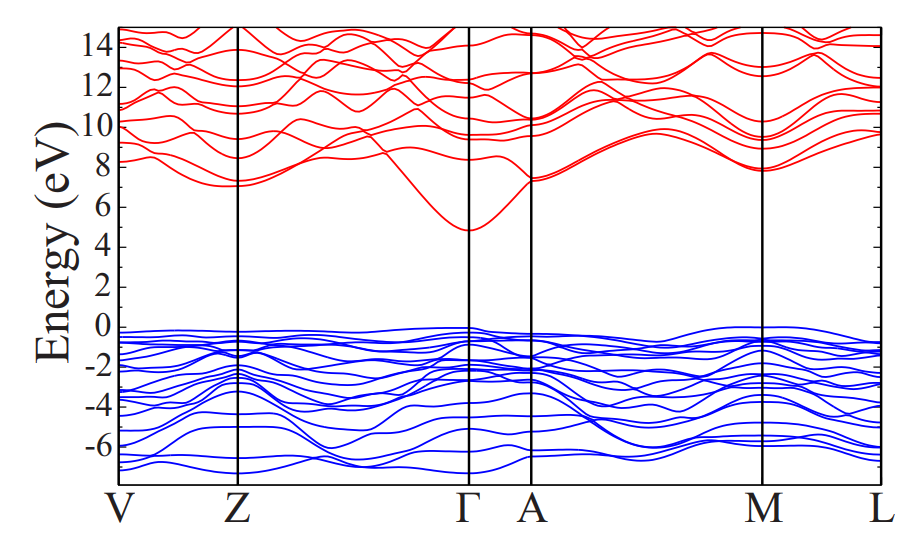
Band structure of β-Gallium Oxide [1].
Faced with this fundamental physical limitation, researchers have not confined themselves to the traditional homojunction p–n junction approach. Instead, they have sought alternative solutions through innovative device architecture design. On one hand, Gallium Oxide power devices are more commonly based on unipolar device architectures, such as Schottky barrier diodes (SBDs), junction field-effect transistors (JFETs), and metal–oxide–semiconductor field-effect transistors (MOSFETs), in order to fully exploit the material’s high critical electric field and low conduction-loss potential.
On the other hand, researchers have explored combining n-type β-Gallium Oxide with p-type conductive wide-bandgap oxides such as nickel oxide (NiO) to form heterojunction p–n structures. This approach introduces p–n-junction-like electric field control without relying on intrinsic p-type doping of Gallium Oxide itself.
Such heterostructures have already been incorporated into several key high-voltage Gallium Oxide device designs, including field-limiting rings (FLRs), junction barrier Schottky (JBS) diodes, and superjunction devices. Through heterojunction band engineering and electric-field distribution optimization, these devices can alleviate edge electric-field crowding, suppress reverse leakage current, and enhance high-voltage blocking capability.
Therefore, heterostructure engineering is not merely a substitute for p-type doping. Rather, it represents a practical and realistic pathway for designing high-voltage Gallium Oxide devices within the current physical limitations of the material system.
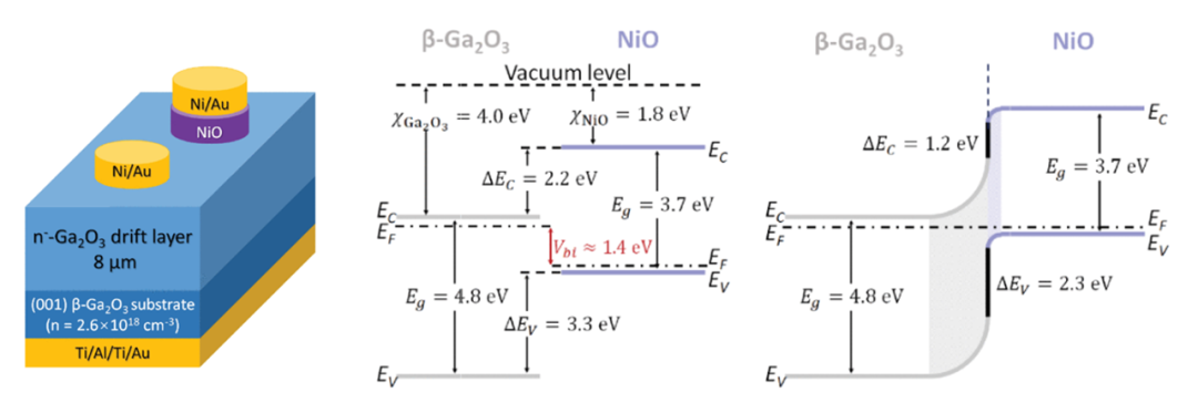
Cross-sectional structure and band alignment mechanism of a high-voltage power device based on a p-NiO/n-Gallium Oxide heterojunction [2].
Reliability Challenges under High Electric Fields:
How to Protect the Gate Dielectric Layer
When focusing on voltage-controlled Gallium Oxide MOSFETs, the high critical breakdown field of β-Gallium Oxide—up to approximately 8 MV/cm—offers tremendous potential for reducing drift region resistance. At the same time, it imposes stricter reliability requirements on the gate dielectric layer. Under high-voltage off-state conditions, the strong internal electric field in Gallium Oxide can concentrate near the device surface and the gate dielectric region, subjecting layers such as Al₂O₃, HfO₂, and SiO₂ to high local electric fields. According to Gauss’s law and the boundary condition of continuous electric displacement, if the dielectric constant of the layer is lower than or comparable to that of Gallium Oxide, the dielectric near the interface may experience a higher field than the semiconductor bulk.
These high interfacial fields can lead to a series of reliability issues, such as increased gate leakage current, enhanced trap charging/discharging at the interface, and, in severe cases, irreversible breakdown of the gate dielectric before the Gallium Oxide itself reaches its breakdown limit. In other words, for Gallium Oxide MOSFETs, the true limit of device voltage capability is often set not by the semiconductor, but by the more vulnerable dielectric and interface regions.
Moreover, the conduction- and valence-band offsets between some dielectrics and β-Gallium Oxide are not ideal, which may fail to fully block high-energy carrier injection, further aggravating gate leakage and long-term reliability degradation. To address this, current research focuses on:
1.Material engineering: Developing high-k or composite dielectrics with suitable permittivity, wide bandgap, and excellent interface quality, while improving film uniformity and reducing interfacial defects using processes such as atomic layer deposition (ALD).
2.Device engineering: Optimizing the electric-field distribution under high-voltage off-state conditions through field-plate structures, trench-gate designs, and shielded source configurations, keeping peak fields away from the gate dielectric and critical interface areas.
Thus, gate dielectric reliability is not merely an interface or process issue—it is a key factor that determines whether the device can truly withstand high voltages and exploit the intrinsic high breakdown field. Achieving a coordinated design of dielectric materials, interfaces, and device architecture to reduce gate-region fields and leakage is essential for enabling high-voltage, high-reliability Gallium Oxide FET applications.
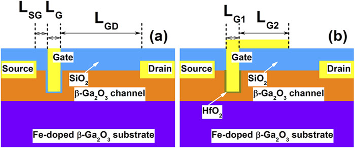
Introduction of high-k dielectric (HfO₂) and field-plate trench-gate in Gallium Oxide MOSFET architecture [3].
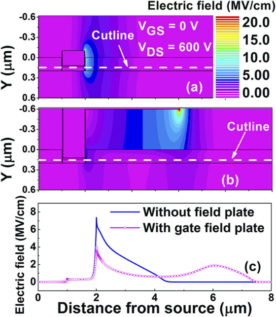
Simulated comparison of electric-field distribution under high-voltage off-state. Advanced field-plate engineering effectively reduces gate peak fields and mitigates time-dependent dielectric breakdown caused by high-field penetration [3].
Multidimensional Thermal Management:
Packaging and Integration to Overcome Intrinsic Material Limits
Beyond challenges in crystal growth, heterostructure design, and high-voltage dielectric reliability, Gallium Oxide faces a critical practical challenge on its path to power device applications—thermal management. As discussed in the previous issue, the room-temperature thermal conductivity of roughly 30 W/m·K is indeed a physical limitation, but it does not invalidate the prospects of Gallium Oxide applications. On the contrary, when the intrinsic thermal properties of a single material cannot fully meet device cooling needs, thermal management must extend beyond the material itself to include device architecture, packaging integration, and system-level heat dissipation design.
The forefront of the industry has keenly recognized the inevitable trend from chip-level to system-level thermal management. In addition to cutting-edge wafer-level heterointegration techniques—such as thinning Gallium Oxide devices to tens of microns and bonding them onto diamond or high-thermal-conductivity SiC substrates—more production-ready packaging solutions are being adapted to the Gallium Oxide ecosystem. These include double-sided cooling modules, active metal-backed ceramic (AMB/DBC) substrates, and top microfluidic channels, which are mature packaging techniques already used in third-generation semiconductor devices.
In this process, tools and strategies such as finite element thermal simulations, interface thermal resistance optimization, chip thinning, backside metallization, and packaging material matching combine to form a systematic solution for Gallium Oxide thermal management. By coordinating materials, devices, packaging, and heat dissipation structures, the self-heating effects of Gallium Oxide devices can be maintained within reasonable limits, allowing the full potential of its high breakdown field and low conduction loss to be realized.
Therefore, low thermal conductivity is not an insurmountable barrier for Gallium Oxide power devices—it is an engineering challenge that must be systematically addressed during industrialization. The extent to which Gallium Oxide can transition from impressive “paper specifications” to high-performance, high-reliability real-world systems will largely depend on the maturity and synchronization of thermal management and packaging integration technologies.
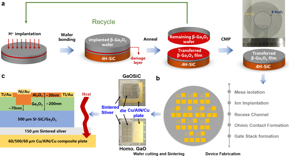
Full-process solution for Gallium Oxide heterointegration and system-level thermal management [4].
Summary of This Issue
How far is Gallium Oxide from becoming the core material of next-generation power devices? A relatively objective answer is: its theoretical limits are already well-defined, while the engineering climb is currently at a critical breakthrough stage.
We must recognize that the industrialization of any frontier material is never instantaneous. Today’s Gallium Oxide is, in some ways, comparable to SiC over a decade ago, when it was gradually overcoming yield, size, and cost bottlenecks—currently in a key transition from materials research to scalable applications. Although the physical limits of p-type doping have not yet been fully resolved, and challenges in dielectric reliability and thermal management remain, Gallium Oxide is steadily translating its intrinsic advantages—4.9 eV ultra-wide bandgap and 8 MV/cm high critical breakdown field—into real-world, ultra-high-voltage, and low-loss devices through multidimensional approaches such as heterojunction band engineering, large-size melt growth, device structure optimization, and system-level packaging and heat dissipation.
As the global industry chain accelerates its closed loop in substrate production, epitaxial growth, and device processing, Gallium Oxide is expected to reshape the landscape of ultra-high-voltage and high-frequency high-power systems, steadily fulfilling its strategic value as the foundation of the new generation of power electronics. What is certain is that this technical marathon—from theoretical potential to industrial reality—has now entered its most critical and closely watched stage.
Referance:
[1] Varley J B, Weber J R, Janotti A, et al. Oxygen vacancies and donor impurities in β-Ga2O3[J]. Applied physics letters, 2010, 97(14).
[2] Lu X, Zhou X, Jiang H, et al. 1 kV sputtered p-NiO/n-Ga2O3 heterojunction diodes with an ultra-low leakage current below μA/cm2[J]. IEEE Electron Device Letters, 2020, 41(3): 449-452.
[3] Do H B, Phan-Gia A V, Nguyen V Q, et al. Optimization of normally-off β-Ga2O3 MOSFET with high Ion and BFOM: A TCAD study. AIP Adv. 2022; 12 (6): 065024.
[4] Qu Z, Xie Y, Zhao T, et al. Extremely low thermal resistance of β-Ga2O3 MOSFETs by co-integrated design of substrate engineering and device packaging[J]. ACS Applied Materials & Interfaces, 2024, 16(42): 57816-57823.
