Paper Sharing
【Member Papers】 Numerical investigation of temperature field and thermal stress of β-Ga₂O₃ crystal by dual heat source coupled laser floating zone method
日期:2026-06-05阅读:58
Researchers from Tianjin University of Technology have published a dissertation titled "Numerical investigation of temperature field and thermal stress of β‑Ga₂O₃ crystal by dual heat source coupled laser floating zone method" in CrystEngComm.
Background
β‑Ga₂O₃ is an ultra‑wide bandgap semiconductor with important applications in high‑power electronics and deep‑ultraviolet photodetectors. The traditional laser floating zone (T‑LFZ) method causes excessive temperature gradient and rapid cooling during β‑Ga₂O₃ growth, leading to severe thermal stress and cracking. Mainstream methods such as EFG, Cz, and VB require expensive noble‑metal crucibles, resulting in high cost. Traditional LFZ lacks active thermal field regulation and cannot effectively suppress thermal stress and crystal cracking. The numerical simulation and regulation mechanism of thermal field and thermal stress for the dual heat source coupled laser floating zone (DHC‑LFZ) method are still unexplored.
Abstract
This study introduces a dual‑heater‑coupled laser floating zone (DHC‑LFZ) system to overcome the severe thermal stress and cracking that plague the growth of β‑Ga₂O₃ single crystals via traditional LFZ methods (T‑LFZ). The key innovation lies in the integration of auxiliary resistance heaters into the T‑LFZ configuration, which allows for active management of the thermal gradient. A multi‑physics finite element model, incorporating coupled phenomena of heat flow, melt convection, interface evolution, radiation, and stress, was established. The results demonstrate that with the introduction of the optimized auxiliary heat source, the DHC‑LFZ system effectively stabilizes the melt–crystal interface, achieving reductions of 46% and 50.5% in the axial and radial temperature gradients, respectively. Consequently, the maximum axial and radial thermal stresses are curtailed by 49.4% and 58.9%, providing a significantly improved crystallization environment. Our work clarifies the underlying mechanisms linking thermal field control to crystal quality and offers a viable path toward the low‑stress growth of large‑sized β‑Ga₂O₃ crystals.
Highlights
Propose a dual‑heater‑coupled laser floating zone (DHC‑LFZ) method to realize active regulation of thermal field for β‑Ga₂O₃ crystal growth via auxiliary resistance heaters
Establish a multi‑physics coupling model of heat conduction‑convection‑radiation‑stress to realize accurate simulation of melt flow and interface morphology
Verify that increasing background temperature can reduce both temperature gradient and thermal stress simultaneously, with maximum axial and radial thermal stress reduced by 49.4% and 58.9% respectively
Reveal a strong linear correlation between temperature gradient and thermal stress, providing quantitative theoretical basis for stress optimization in wide‑bandgap semiconductor crystal growth
Conclusion
This study established a comprehensive multi‑physics model to simulate β‑Ga₂O₃ crystal growth, comparing the T‑LFZ and novel DHC‑LFZ systems. The work clarifies the impact of different thermal field designs on heat transfer, melt flow, interface morphology, and thermal stress, and quantitatively demonstrates the control mechanism of the BT for the DHC‑LFZ system. The key findings are as follows:
(1) The dual‑heater design of the DHC‑LFZ system fundamentally optimizes the growth environment. It enhances thermal field uniformity by reducing the axial temperature difference, suppresses melt flow by lowering the radial temperature gradient, and dynamically stabilizes the phase‑change interface, ultimately leading to a significant reduction in crystal thermal stress.
(2) Increasing the BT effectively moderates the melt zone. The maximum melt temperature decreases by 102 K, and the flow velocity drops by 39.9%. Due to the combined effects of reconstructed thermodynamic equilibrium, a suppressed Marangoni effect, and the Gibbs–Thomson effect, the curvatures of the melt–rod and melt–crystal interfaces are reduced by 30.5% and 18.0%, respectively, driving the system toward a more stable, planar interface configuration.
(3) The DHC‑LFZ system achieves a remarkable suppression of thermal stress. The maximum axial and radial temperature gradients are reduced by 46% and 50.5%, respectively. This directly leads to a corresponding decrease of 49.4% and 58.9% in the maximum axial and radial thermal stresses. The expansion of the low‑stress region in the crystal body significantly mitigates the risk of cracking.
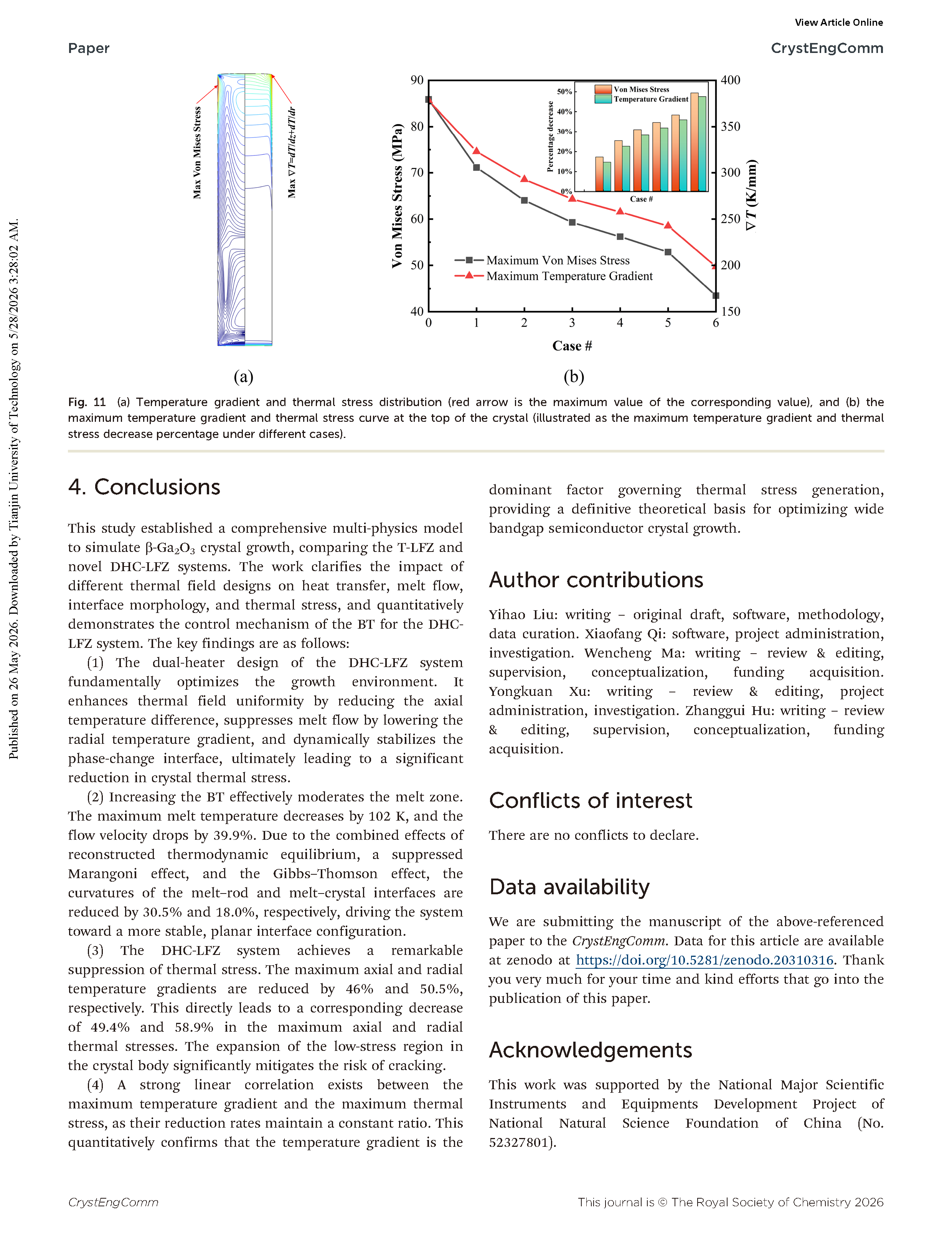
(4) A strong linear correlation exists between the maximum temperature gradient and the maximum thermal stress, as their reduction rates maintain a constant ratio. This quantitatively confirms that the temperature gradient is the dominant factor governing thermal stress generation, providing a definitive theoretical basis for optimizing wide bandgap semiconductor crystal growth.
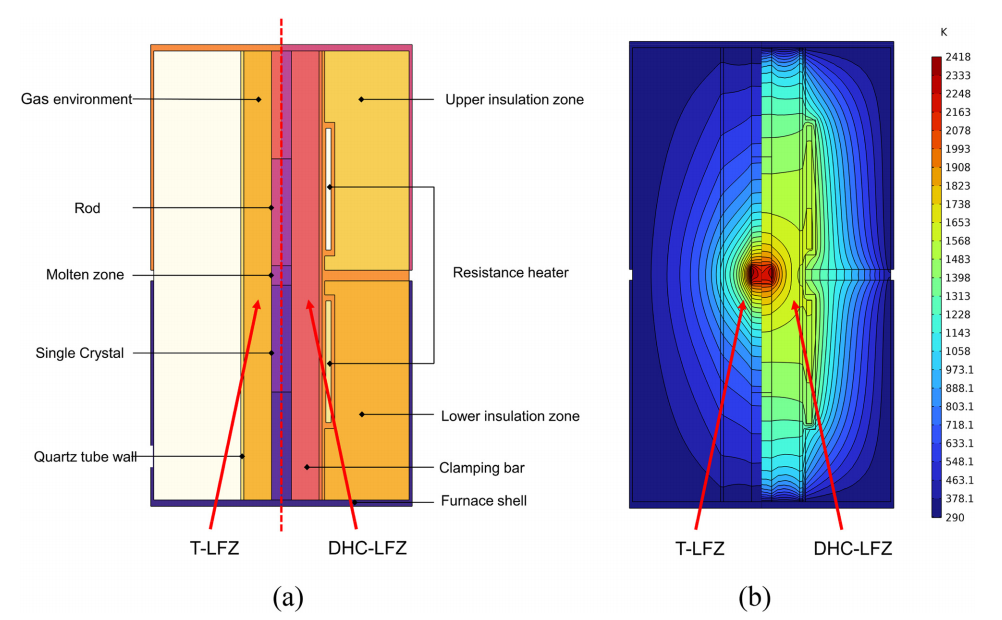
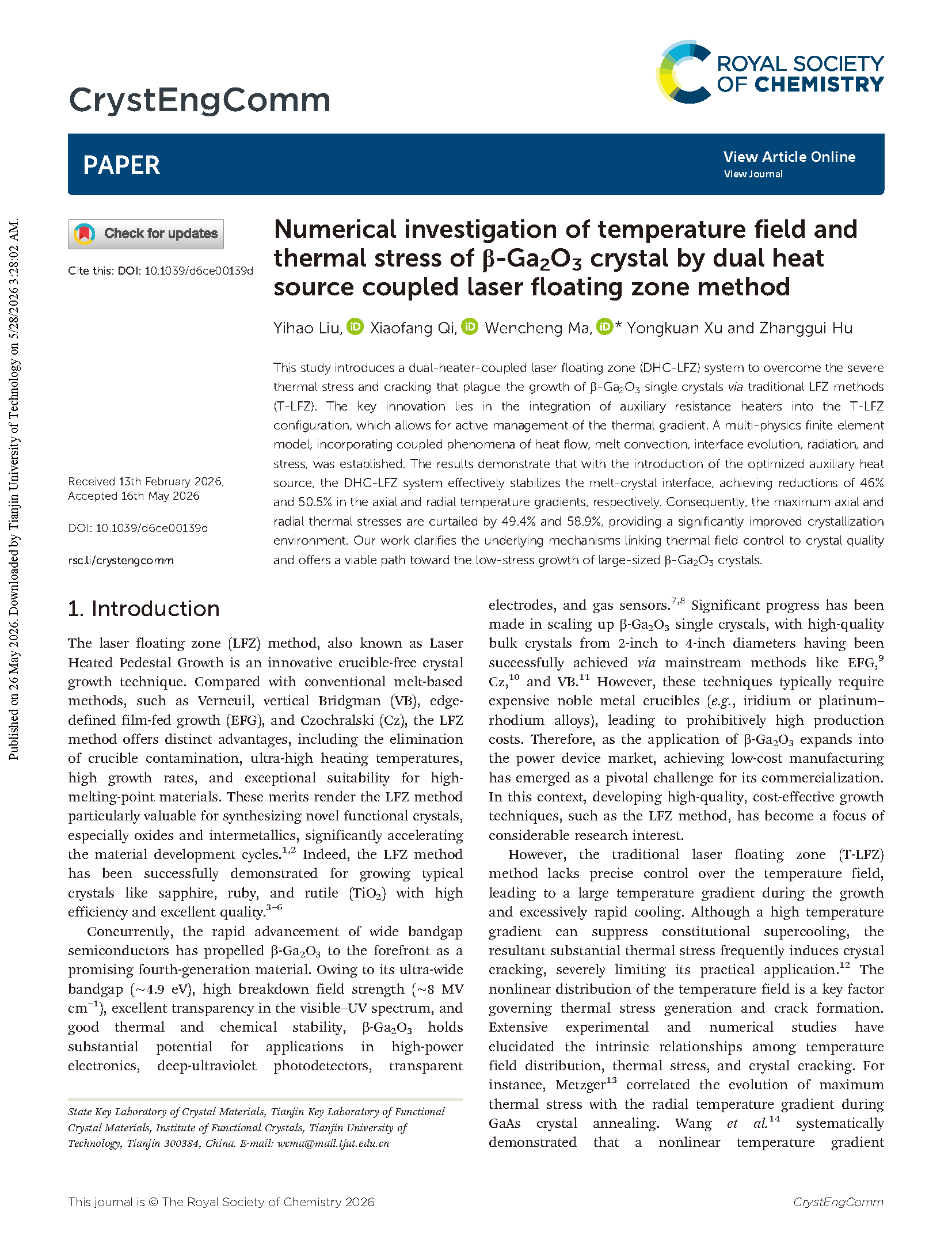
Fig. 1 (a) Physical model diagram and (b) global thermal field distribution.
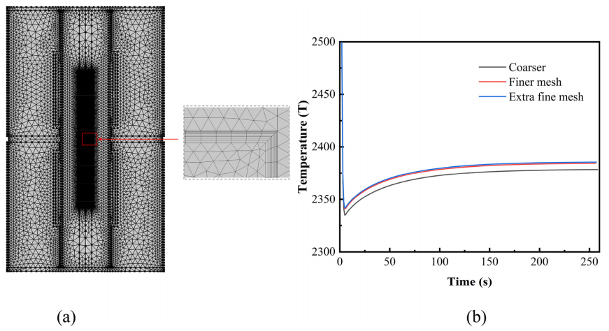
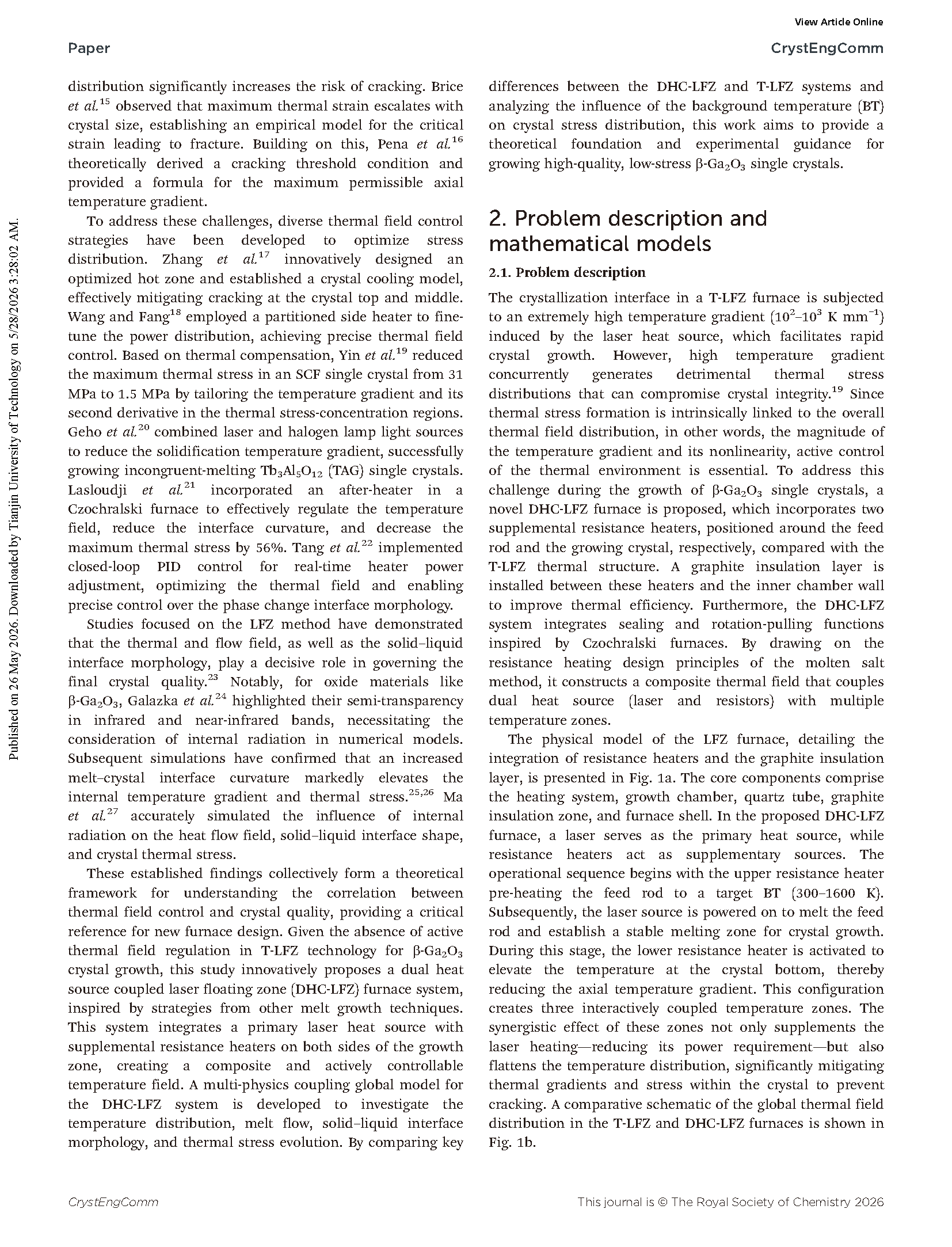
Fig. 2 (a) Meshing of the calculation model and (b) the time–temperature curves of the model under three grid divisions.
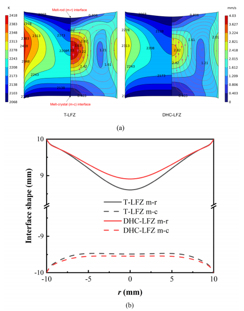
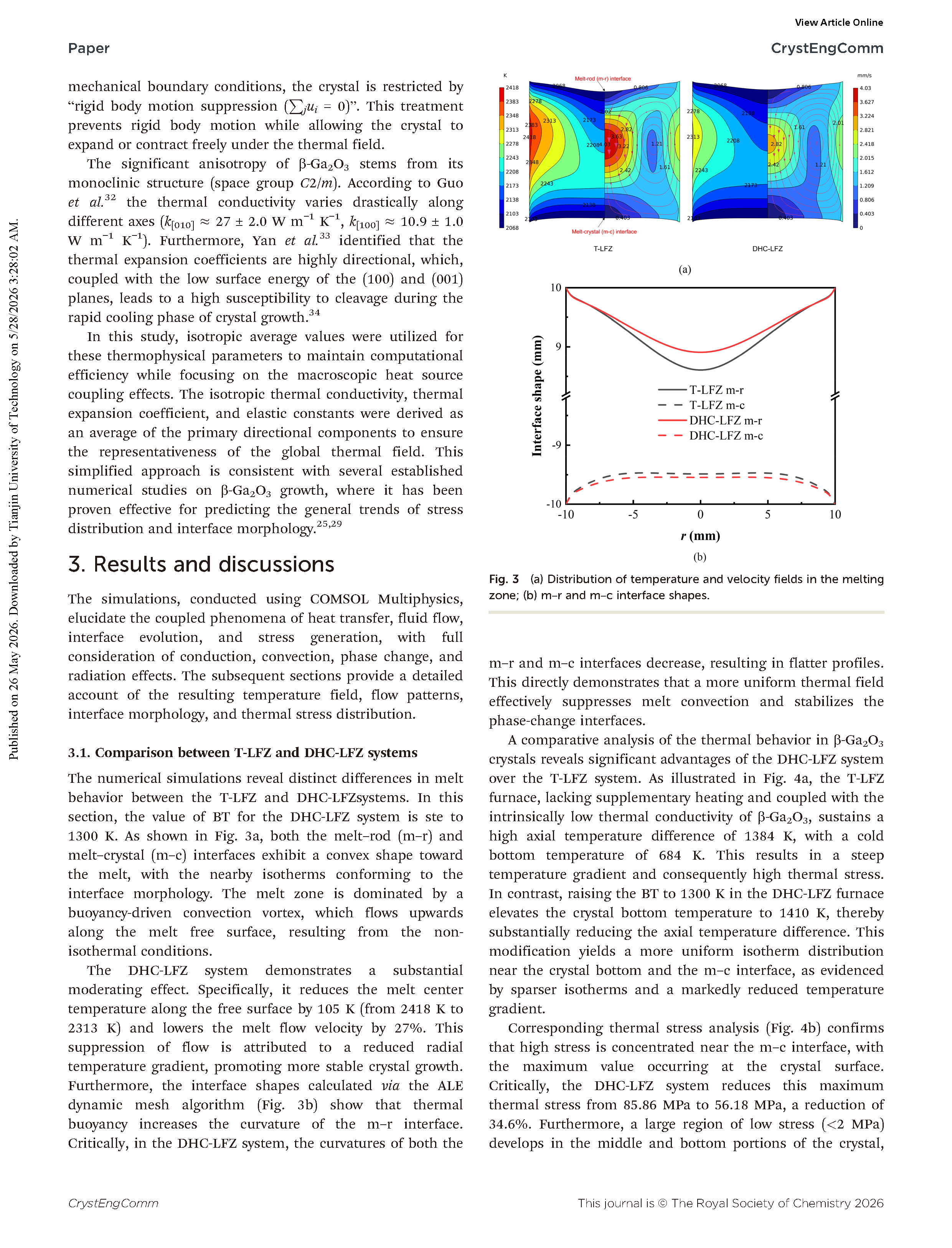
Fig. 3 (a) Distribution of temperature and velocity fields in the melting zone; (b) m–r and m–c interface shapes.
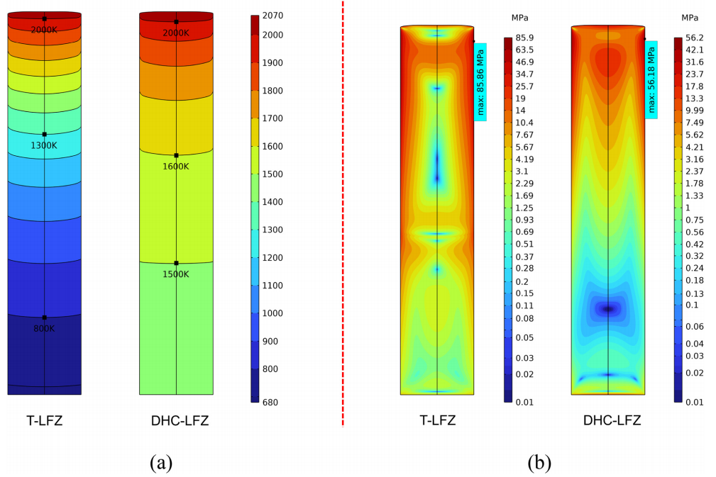
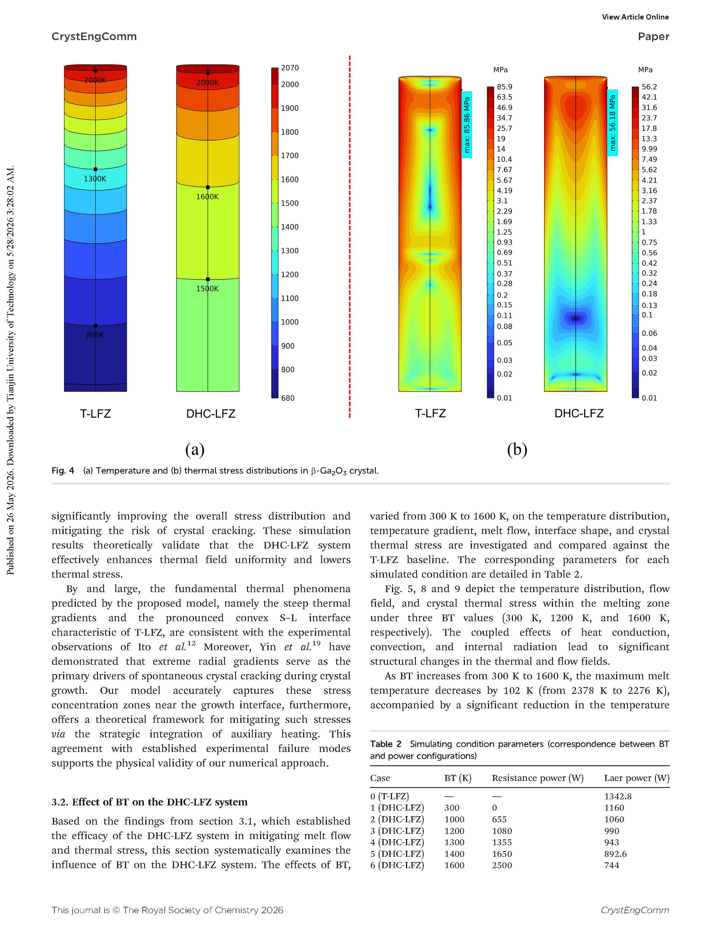
Fig. 4 (a) Temperature and (b) thermal stress distributions in β‑Ga₂O₃ crystal.
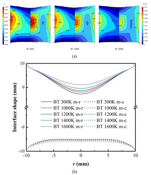
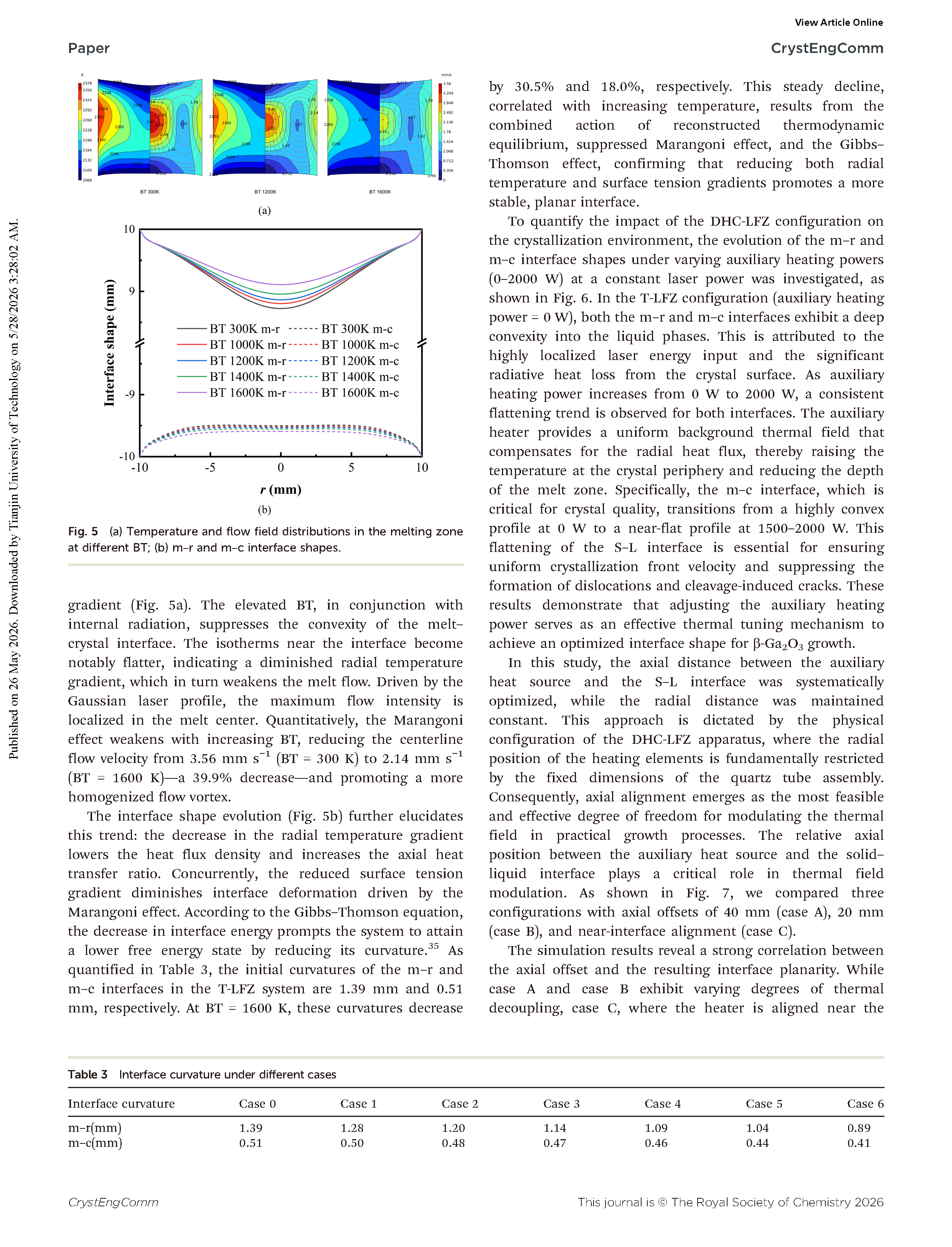
Fig. 5 (a) Temperature and flow field distributions in the melting zone at different BT; (b) m–r and m–c interface shapes.
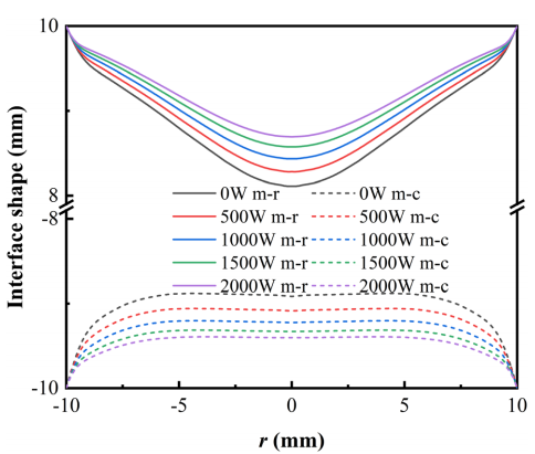
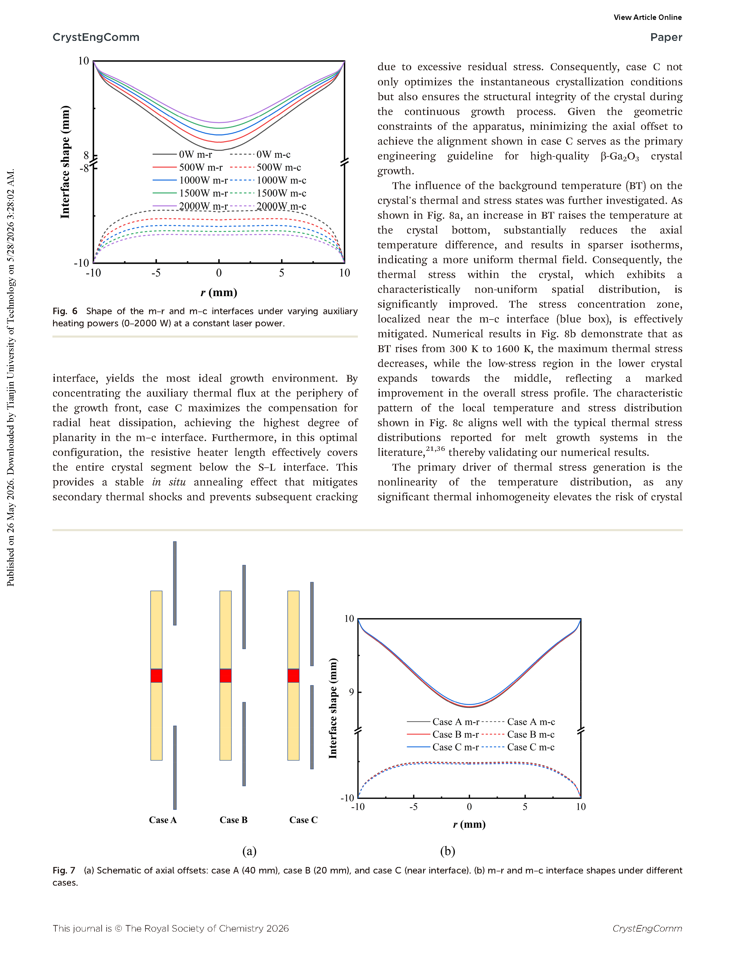
Fig. 6 Shape of the m–r and m–c interfaces under varying auxiliary heating powers (0–2000 W) at a constant laser power.
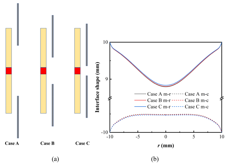
Fig. 7 (a) Schematic of axial offsets: case A (40 mm), case B (20 mm), and case C (near interface). (b) m–r and m–c interface shapes under different cases.
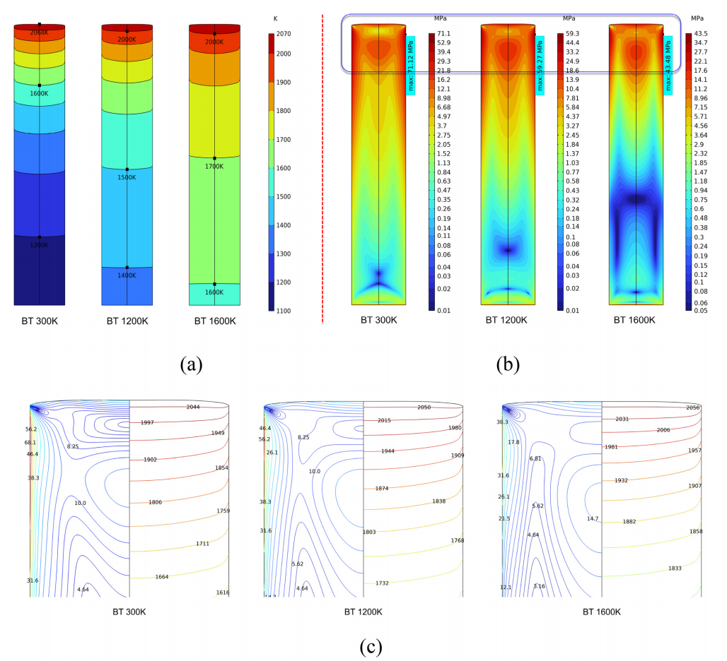
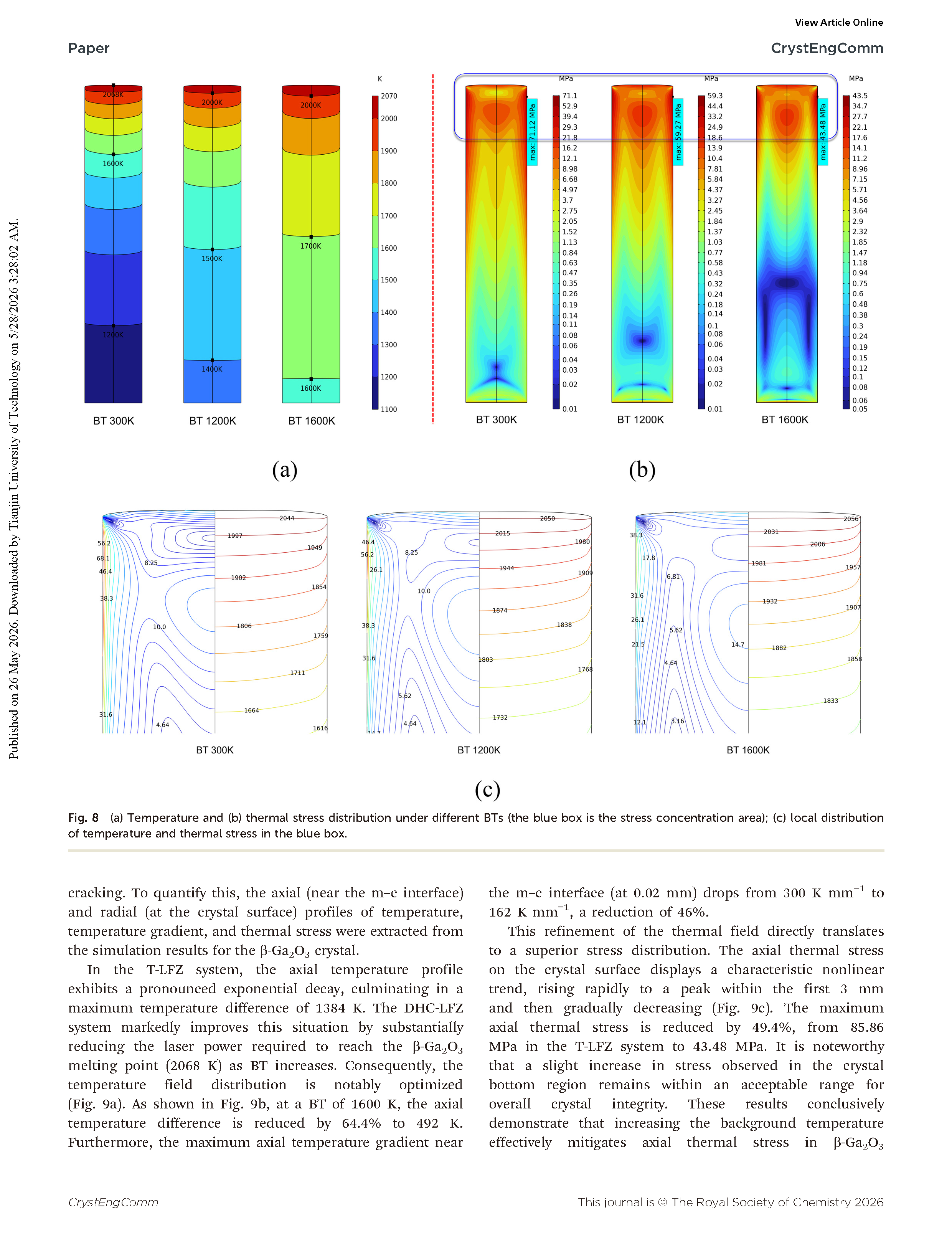
Fig. 8 (a) Temperature and (b) thermal stress distribution under different BTs (the blue box is the stress concentration area); (c) local distribution of temperature and thermal stress in the blue box.
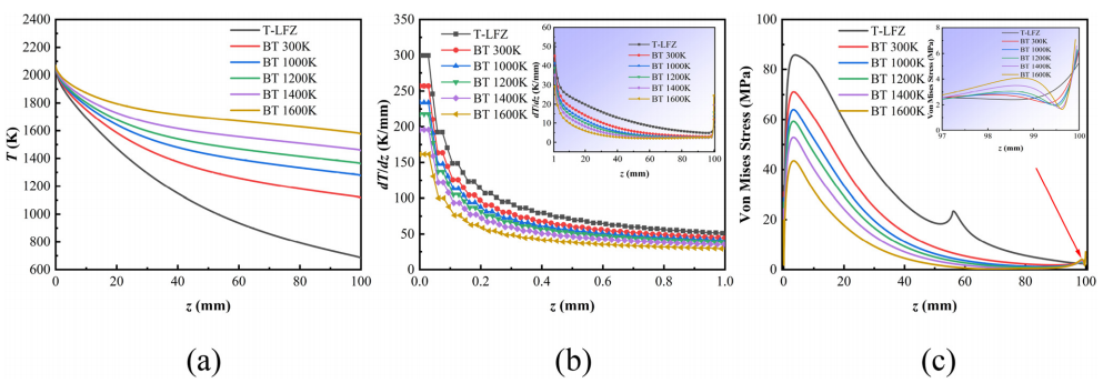
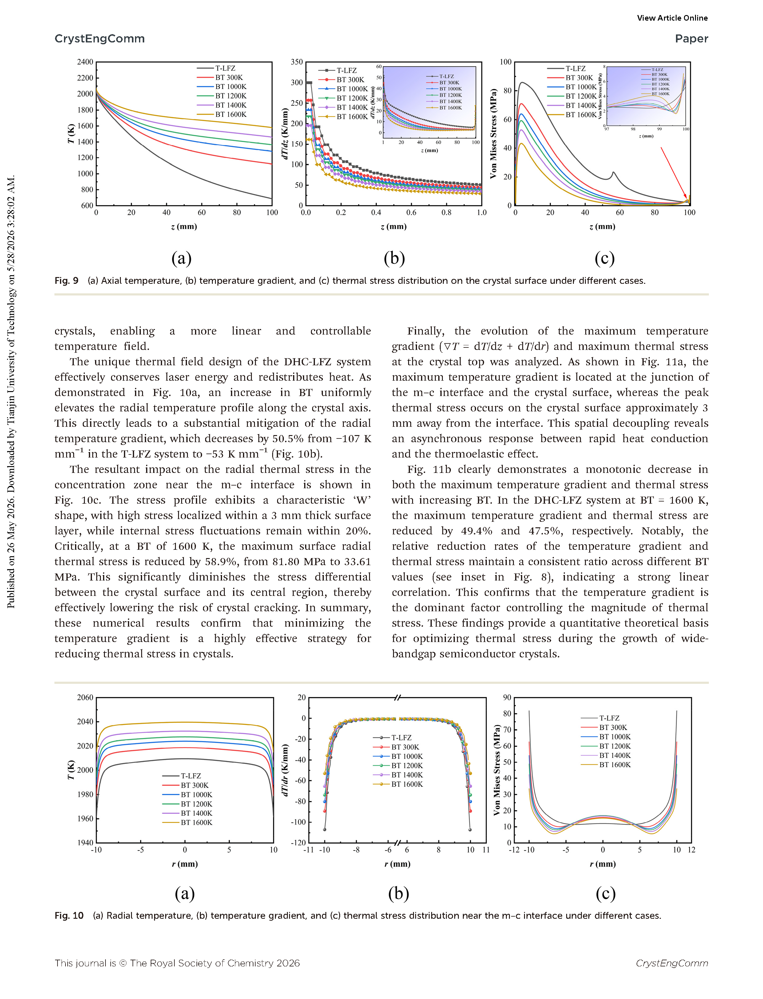
Fig. 9 (a) Axial temperature, (b) temperature gradient, and (c) thermal stress distribution on the crystal surface under different cases.
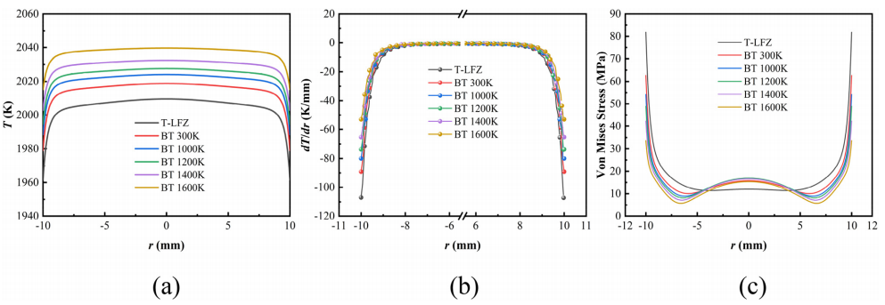
Fig. 10 (a) Radial temperature, (b) temperature gradient, and (c) thermal stress distribution near the m–c interface under different cases.
DOI:
doi.org/10.1039/d6ce00139d