Member News
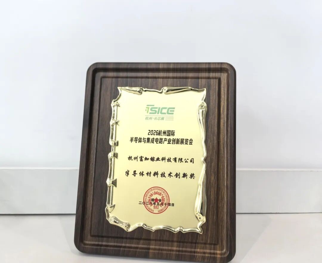
【Member News】Good News! Fujia Gallium Awarded the “Semiconductor Materials Technology Innovation Award”
日期:2026-06-01阅读:74
On May 14, 2026, at the International Semiconductor and Integrated Circuit Industry Innovation Exhibition (referred to as "IC-Show") in Hangzhou, Hangzhou Fujia Gallium Technology Co., Ltd. (hereinafter referred to as "Fujia Gallium") won the "Semiconductor Material Technology Innovation Award" for its core breakthroughs in the field of ultra-wide bandgap semiconductor gallium oxide. This is not only an authoritative recognition of Fujia Gallium's outstanding achievements in recent years, but also the most resounding endorsement of the "Fujia Speed."
Gallium Oxide Industry Races Forward at "Fujia Speed"
Starting from scratch to achieving global leadership, Fujia Gallium has written a legendary tale of the rise of China's gallium oxide industry in less than seven years.
2019
·Foundation: Fujia Gallium was established with a clear and resolute vision: to master the entire gallium oxide industry chain and drive its large-scale application across power devices, microwave RF, and photodetectors.
2021
·Pioneering Innovation: Pioneered the research of AI-assisted single crystal growth and seized a commanding height in global intellectual property, securing 14 international patents authorized across the United States, Japan, and the European Union.
2022
·Epitaxial Breakthroughs: Concurrently deployed MOCVD and MBE epitaxial technologies, becoming the only domestic supplier capable of providing MBE epi-wafers.
·Media Recognition: Achieved a breakthrough in "one-click crystal growth" technology and equipment, which was later featured on CCTV-1 in 2024, laying a solid foundation for industrial commercialization.
2023
·Dual-Route Strategy: Pioneered the introduction of the Vertical Bridgman (VB) method for Ga₂O₃ single crystal growth, successfully expanding its technological portfolio from a single EFG route to a dual-method parallel approach.
2024
·Industry Firsts: Successfully grew China's first conductive 6-inch single crystal using the Edge-defined Film-fed Growth (EFG) method.
·Technical Milestones: Achieved consecutive domestic-first breakthroughs in growing 3-inch and 4-inch Ga single crystals via the VB method.
·Capacity Expansion: Commenced construction on China's first production line with an annual capacity of 10,000 6/8-inch Ga₂O₃ single crystals and epi-wafers.
2025
·Global Leadership: Unveiled the world’s largest 6-inch and 8-inch Ga₂O₃ single crystals grown by the VB method.
·Technical Perfection: Made a major breakthrough in MOCVD homoepitaxial technology, preparing epi-wafers with thicknesses exceeding 10 um and a world-leading mobility of 181.6 cm2/V·s.
·Standard Setting: Led the drafting of China's first national standard in the gallium oxide field: Gallium Oxide Single Crystal Polished Wafers.
2026
·Breaking World Records: Shocked the industry with the debut of the world’s very first 12-inch Ga₂O₃ single crystal.
D·ownstream Integration: Collaborated with downstream users to introduce China's first chip-level packaged and tested Ga₂O₃ diode devices.
Record-Setting Performance: Its self-developed homoepitaxial wafers empowered Jiufengshan Laboratory to develop a lateral Ga₂O₃ MOSFET device with a breakdown voltage exceeding 9000V, shattering the world record!
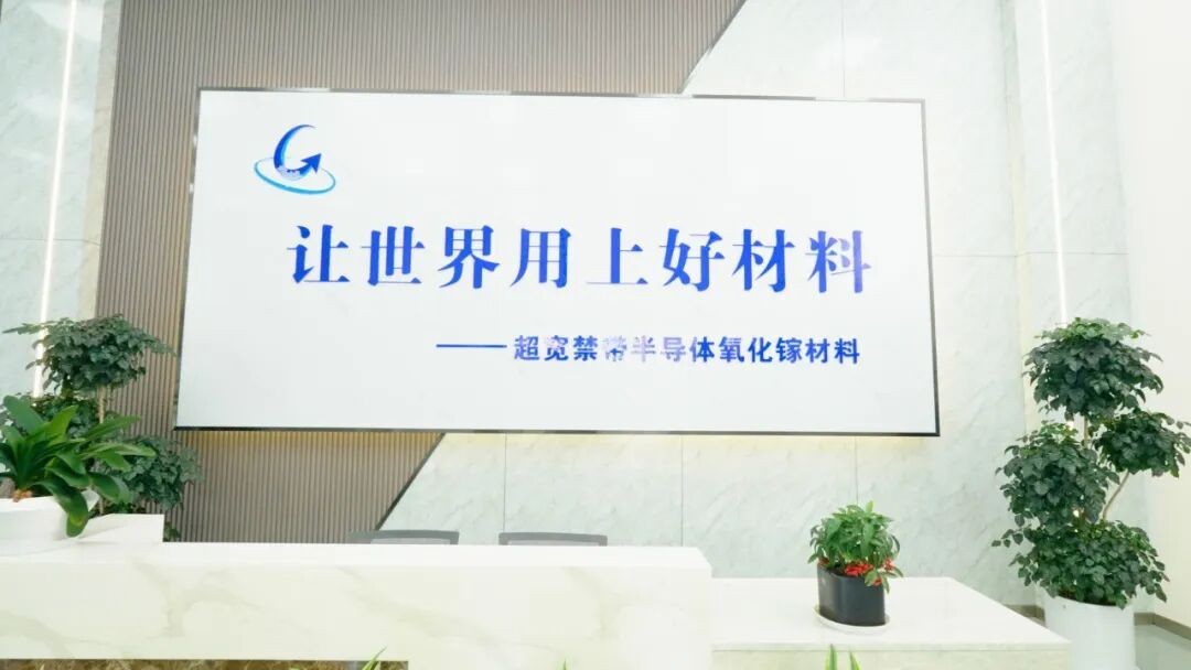
The endless pursuit: "Equipping the world with superior materials."
Through one groundbreaking milestone after another, Fujia Gallium is resoundingly answering the most profound call of our era.