


Discover
【Knowledge Discover】Decoding Gallium Oxide: Where Its Advantages Come From and Where Its Limits Lie
日期:2026-05-29阅读:122
Introduction:
In the previous two issues, we explored gallium oxide from the perspectives of material positioning and crystal structure. We learned that it is not only a highly promising ultra-wide bandgap semiconductor but also possesses diverse crystal phases and unique structural features.
In the fields of power electronics and optoelectronic devices, the performance limits of a material are largely determined by fundamental parameters such as bandgap, critical breakdown field, electron mobility, and thermal conductivity. As the demand for high voltage tolerance, low loss, and high power density continues to grow, traditional semiconductors are approaching their intrinsic performance ceilings. Even wide-bandgap semiconductors like 4H-SiC and GaN exhibit performance boundaries dictated by their inherent parameters when pushed to higher power densities and more extreme operating conditions.
Against this backdrop, ultra-wide bandgap semiconductors such as β-Ga₂O₃ and diamond have attracted widespread attention. β-Ga₂O₃, in particular, demonstrates significant potential for next-generation power and deep-ultraviolet optoelectronic devices, thanks to its ultra-wide bandgap, high theoretical breakdown field, and the ability to grow large single crystals via the melt method.
So, what are the key parameters that define the advantages of β-Ga₂O₃? Beyond its high breakdown field, what intrinsic limitations does it have? In this issue, we will systematically analyze the “performance ID” of β-Ga₂O₃, starting from its fundamental physical parameters.
Issue 3
The “Performance ID” of Gallium Oxide:
Understanding Its Key Physical Parameters at a Glance
Starting from Key Parameters:
Understanding the Material Potential of β-Ga₂O₃
Evaluating the application potential of a semiconductor material in power electronics cannot rely on a single parameter alone. Instead, it requires a comprehensive consideration of key intrinsic properties, including band structure, dielectric characteristics, carrier transport capability, and thermal transport performance.
Among the many polymorphs of gallium oxide, β-Ga₂O₃, which belongs to the monoclinic crystal system, is currently the most extensively studied phase and the only thermodynamically stable phase under ambient conditions.
More importantly, β-Ga₂O₃ can be grown into large bulk single crystals using melt-growth methods similar to those used for silicon. This feature provides unique advantages in substrate preparation, wafer scaling, and manufacturing cost control, forming a key industrialization advantage that distinguishes it from wide-bandgap semiconductors such as SiC and GaN.
The table below systematically compares the key room-temperature physical parameters of β-Ga₂O₃ with representative semiconductor materials including Si, GaAs, 4H-SiC, GaN, and diamond.
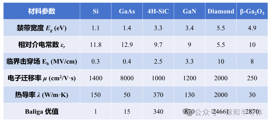
Table 1. Comparison of Key Room-Temperature Physical Parameters of β-Ga₂O₃ and Major Semiconductor Materials [1]
From the table, it is evident that the most prominent advantages of β-Ga₂O₃ lie in its ultra-wide bandgap and high theoretical critical breakdown field. Its breakdown field strength is significantly higher than that of Si, GaAs, 4H-SiC, and GaN, second only to diamond. At the same time, its Baliga’s figure of merit is far superior to that of conventional semiconductors and typical wide-bandgap semiconductors, indicating that β-Ga₂O₃ holds considerable theoretical potential for high-voltage, low-on-resistance power devices.
Bandgap (Eg):
A Key Parameter Governing High-Temperature Tolerance and Deep-UV Response
The bandgap (Eg) is the energy difference between the top of the valence band and the bottom of the conduction band in a semiconductor, representing the minimum energy required for electrons to transition from the valence band to the conduction band and become free carriers. For semiconductor devices, the bandgap is one of the fundamental parameters that determines intrinsic thermal stability, radiation resistance, and photoelectric absorption characteristics.
Under high-temperature conditions, thermally excited carriers are generated inside semiconductors. If the concentration of these carriers becomes too high, the device off-state leakage current increases significantly and may even weaken its blocking capability. Therefore, a wider bandgap generally enables stronger suppression of intrinsic thermal excitation, providing a more favorable material foundation for stable operation under high-temperature and high-voltage conditions.
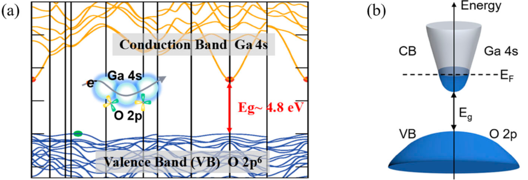
(a) Band structure of β-Ga₂O₃ calculated using hybrid density functional theory.
(b) Energy-level diagram of Ga₂O₃, showing the conduction band (CB) derived from Ga 4s orbitals and the valence band (VB) derived from O 2p orbitals [2].
From this perspective, β-Ga₂O₃ possesses remarkable intrinsic advantages. At room temperature, its bandgap is approximately 4.9 eV, far wider than that of conventional Si (1.1 eV), and also significantly larger than those of 4H-SiC (3.3 eV) and GaN (3.4 eV). According to the relationship between intrinsic carrier concentration and bandgap, a larger bandgap can greatly reduce the concentration of thermally generated carriers. This means that even at elevated temperatures, β-Ga₂O₃ is expected to maintain low intrinsic carrier concentration and low off-state leakage current, providing important support for high-temperature and high-voltage power device applications.
In addition, a bandgap of about 4.9 eV corresponds to an absorption cutoff wavelength of approximately 250 nm, which lies in the deep-ultraviolet region. As a result, β-Ga₂O₃ is essentially insensitive to visible light while exhibiting effective absorption in the solar-blind UV range. Therefore, beyond power electronics, β-Ga₂O₃ is also regarded as an important candidate material for solar-blind deep-UV photodetectors.
Relative Dielectric Constant (εr):
A Key Parameter Influencing Electric-Field Control and Device Capacitance
The relative dielectric constant (εr) reflects a material’s ability to polarize in response to an external electric field—that is, how the bound charges inside the material respond to the applied field and, to some extent, weaken the local electric field. For power semiconductor devices, the dielectric constant significantly affects electric-field distribution, depletion-region capacitance, and dynamic switching characteristics.
On one hand, a higher dielectric constant generally leads to larger junction and parasitic capacitances, increasing charge–discharge losses during high-frequency switching. On the other hand, it also influences the electric-field distribution in device terminals, helping mitigate edge-field crowding and improving voltage-withstanding margins. Therefore, the dielectric constant is not simply “the higher the better” or “the lower the better”; it must be considered in conjunction with device structure, operating frequency, and voltage requirements.
For β-Ga₂O₃, the relative dielectric constant (defined as the ratio of the material’s dielectric constant to that of vacuum) is approximately 10. This is close to 4H-SiC, lower than Si and GaAs, and higher than diamond. Overall, β-Ga₂O₃’s dielectric constant is moderate: it supports effective electric-field control in high-voltage devices without significantly increasing device capacitance. For Ga₂O₃ power devices, this parameter provides a favorable material foundation for high-voltage structure design.
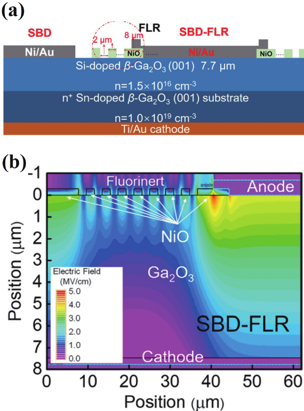
(a) Cross-sectional schematic of a β-Ga₂O₃ power device using a field-limiting ring terminal structure.
(b) Simulated 2D electric-field distribution in the device under high-voltage blocking conditions.
Intrinsic parameters like the relative dielectric constant directly determine the ability to smooth and expand terminal-region electric fields and to mitigate field-crowding effects.
Critical Breakdown Field (Eb):
A Key Parameter Determining Voltage Withstand and Device Scaling Potential
The critical breakdown field (Eb) refers to the maximum electric field a semiconductor material can withstand before avalanche breakdown occurs. For power devices, it is a key parameter used to evaluate voltage-blocking capability and device scaling potential. In general, the higher the critical breakdown field, the thinner the drift layer required to sustain the same blocking voltage, enabling devices to achieve lower on-resistance under high-voltage operation.
β-Ga₂O₃ has a bandgap of approximately 4.9 eV. This large bandgap raises the energy threshold required for carrier impact ionization, allowing the material to withstand much higher internal electric fields without triggering avalanche breakdown. As a result, the theoretical critical breakdown field of β-Ga₂O₃ can reach around 8 MV/cm, significantly higher than that of Si (0.3 MV/cm), GaAs (0.4 MV/cm), 4H-SiC (2.5 MV/cm), and GaN (3.3 MV/cm).
For high-voltage power devices, the high critical breakdown field of β-Ga₂O₃ is considered one of its most competitive core advantages. A theoretical breakdown field of approximately 8 MV/cm means that, at the same voltage rating, β-Ga₂O₃ devices can employ much thinner drift layers than Si, SiC, and GaN devices. This greatly shortens carrier transport paths, reduces drift-region resistance, and enables more compact device structures. Since drift-region resistance is typically one of the major contributors to conduction loss in high-voltage unipolar power devices, β-Ga₂O₃ has the potential to achieve a superior balance between high voltage capability and low conduction loss. This is also one of the main reasons why gallium oxide is regarded as a promising candidate for breaking through the performance limits of conventional wide-bandgap semiconductors and enabling next-generation high-voltage power devices.
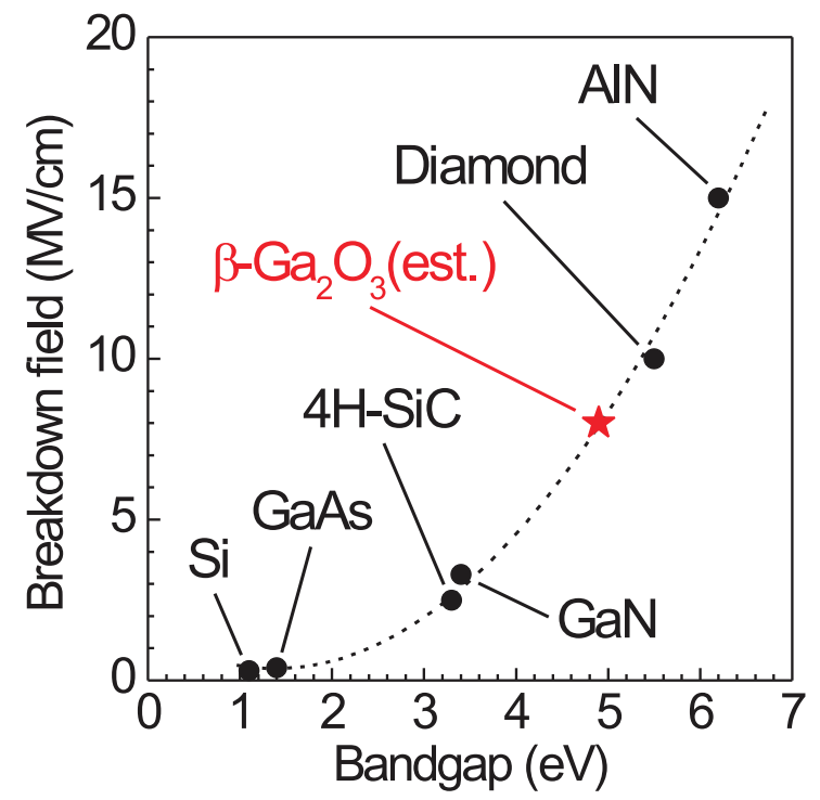
Strong positive correlation between semiconductor critical breakdown field (Eb) and bandgap width (Eg) [4].
It should be noted that a high theoretical breakdown field does not necessarily mean that a device can achieve the same level of actual breakdown performance. In practical devices, voltage-blocking capability is also affected by factors such as defect density, edge termination design, interface states, electric-field crowding, and thermal management. Therefore, while the high breakdown field of β-Ga₂O₃ provides an excellent material foundation for high-voltage power devices, fully translating this advantage into device performance still requires coordinated optimization of epitaxial quality, device structure, and process reliability.
Electron Mobility (μ) and Baliga FOM:
Key Metrics for Evaluating Conduction Loss Potential
Electron mobility (μ) is defined as the average drift velocity of conduction-band electrons under a unit electric field. It directly reflects the efficiency of carrier transport and is a key physical parameter affecting device on-resistance and switching speed. Generally, higher electron mobility allows carriers to move more easily through the material, potentially reducing conduction loss in the device.
However, for high-voltage unipolar power devices, electron mobility alone cannot fully indicate the material's conduction loss limits. Compared to simply comparing mobility, the Baliga Figure of Merit (BFOM) integrates carrier transport capability, electric-field tolerance, and depletion-region control into a unified evaluation, more accurately reflecting the theoretical low-loss potential of a material in high-voltage unipolar devices.
The Baliga FOM does not simply multiply a few material parameters; it originates from the fundamental trade-off between voltage-blocking capability and on-resistance in high-voltage unipolar devices. In ideal devices, the main on-resistance comes from the drift region, which must be thick and lightly doped to withstand high voltage, yet thin and more heavily doped to minimize resistance. Under a one-dimensional ideal approximation, the theoretical specific on-resistance is proportional to the square of the blocking voltage and inversely proportional to the cube of the critical breakdown field, electron mobility, and relative permittivity, i.e., BFOM ∝ εr·μ·Eb³.
Looking at individual parameters, Ga₂O₃ shows an intrinsic disadvantage in electron mobility. Due to strong polar optical phonon scattering at the conduction-band minimum, its room-temperature mobility is only ~250 cm²/V·s, far below GaAs (~8000 cm²/V·s) and 4H-SiC (~1000 cm²/V·s). However, the weighting of parameters in the BFOM formula highlights a striking fact: the breakdown field Eb dominates with a cubic influence. With a high theoretical breakdown field of 8 MV/cm, the cubic scaling completely offsets Ga₂O₃’s lower mobility.
Using silicon’s BFOM as 1 for reference, 4H-SiC achieves 340, GaN reaches 870, and β-Ga₂O₃ reaches an astonishing 2870. This demonstrates that, despite slower carrier transport, Ga₂O₃ devices can exploit thinner drift regions under the same voltage rating, reducing theoretical conduction loss to a fraction of third-generation semiconductors, revealing outstanding energy-saving and efficiency potential.
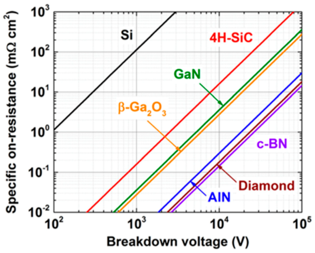
Plot of Specific On-Resistance versus Breakdown Voltage for Various Semiconductors [5]
Thermal Conductivity (λ):
Microscopic Phonon Scattering Mechanisms and Thermal Management Considerations
Thermal conductivity (λ) describes a material’s ability to transfer heat. In semiconductors, heat is mainly transported through lattice vibrations, namely phonon transport. For high-power devices, thermal conductivity directly affects whether Joule heat generated during continuous operation can be dissipated efficiently, making it an important parameter for evaluating device thermal stability and reliability.
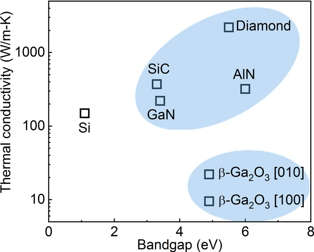
As shown in Table 1, β-Ga₂O₃ demonstrates outstanding advantages in breakdown field strength and theoretical low-loss potential, but its heat transport capability is relatively weak. Due to its low-symmetry monoclinic crystal structure, the unit cell contains a large number of atoms and exhibits complex lattice vibration modes, resulting in strong phonon scattering. Consequently, the room-temperature thermal conductivity of β-Ga₂O₃ is relatively low, around 30 W/m·K. In comparison, 4H-SiC has a thermal conductivity of approximately 370 W/m·K, Si about 150 W/m·K, and diamond can reach nearly 2000 W/m·K. Therefore, low thermal conductivity is regarded as one of the intrinsic limitations of β-Ga₂O₃ for power device applications.
Under practical high-voltage, high-current, or high-frequency operating conditions, poor thermal conductivity can easily lead to heat accumulation inside the device, causing self-heating effects. Elevated temperature not only affects electron mobility and on-resistance, but may also accelerate defect evolution, interface degradation, and reliability deterioration. As a result, thermal management is widely considered one of the key challenges limiting further improvements in power density and long-term stability of β-Ga₂O₃ power devices.
Room-Temperature Thermal Conductivity of Typical Semiconductor Materials [6]
However, a low thermal conductivity does not mean that gallium oxide loses its application value. On the contrary, it motivates researchers to explore solutions at the device structure and packaging level. For example, by thinning the substrate, transferring the device layer, employing heterogeneous integration, implementing backside heat-spreading structures, or bonding with high-thermal-conductivity materials, the thermal transport path can be shortened and the device’s heat dissipation capability enhanced. In particular, combining the β-Ga₂O₃ active layer with high-thermal-conductivity substrates such as diamond or SiC is considered an important engineering route to mitigate self-heating effects.
Therefore, the thermal conductivity limitation of β-Ga₂O₃ is not a negligible issue; it represents a key technical challenge that must be addressed as the material transitions from intrinsic advantages to practical device applications. The extent to which β-Ga₂O₃ power devices can fully realize their high breakdown field and low theoretical conduction loss potential largely depends on the synergistic optimization of epitaxial quality, device structural design, and advanced thermal management technologies.
Summary of This Issue
A careful examination of the parameter profile of gallium oxide (β-Ga₂O₃) leads to a clear physical conclusion: gallium oxide is not a perfectly balanced material in every aspect, but rather a highly distinctive “specialized talent.” Its ultra-wide bandgap of 4.9 eV and theoretical critical breakdown field of approximately 8 MV/cm provide an exceptionally strong foundation for high-voltage operation, while its remarkable Baliga FOM of up to 2870 offers significant theoretical potential for surpassing the loss limits of existing power devices.
Although its complex crystal structure results in less-than-ideal electron mobility and thermal conductivity, the extremely high breakdown field grants devices much greater design flexibility. Through approaches such as ultra-thin drift-layer design, substrate thinning, heterogeneous integration, and thermal management assisted by high-thermal-conductivity materials like diamond, researchers are actively exploring engineering solutions to mitigate these intrinsic limitations.
With continued advances in material growth, defect control, device architecture, and thermal management technologies, gallium oxide is expected to unlock even greater potential in next-generation ultra-wide-bandgap semiconductor devices.
References:
[1] Chabak K D, Leedy K D, Green A J, et al. Lateral β-Ga2O3 field effect transistors[J]. Semiconductor Science and Technology, 2020, 35(1): 013002.
[2] Xu W, Chen Y, Zhou X, et al. Recent advancement and perspective of epitaxial growth and doping of β-Ga2O3 thin films for power electronics[J]. APL Materials, 2025, 13(10).
[3] Lu X, Deng Y, Pei Y, et al. Recent advances in NiO/Ga2O3 heterojunctions for power electronics[J]. Journal of Semiconductors, 2023, 44(6): 061802.
[4] Higashiwaki M, Sasaki K, Kuramata A, et al. Gallium oxide (Ga2O3) metal-semiconductor field-effect transistors on single-crystal β-Ga2O3 (010) substrates[J]. Applied Physics Letters, 2012, 100(1).
[5] Pearton S J, Aitkaliyeva A, Xian M, et al. Radiation damage in wide and ultra-wide bandgap semiconductors[J]. ECS Journal of Solid State Science and Technology, 2021, 10(5): 055008.
[6] Cheng Z, Shi J, Yuan C, et al. Thermal science and engineering of β-Ga2O3 materials and devices[M]//Semiconductors and Semimetals. Elsevier, 2021, 107: 77-99.
