


Member News
【Member News】Major Scientific Research Breakthrough | Garen Semiconductor Empowers Shenzhen Pinghu Laboratory Team to Achieve a Leapfrog Breakthrough in Gallium Oxide Photoconductive Switches
日期:2026-05-27阅读:138
Recently, the Fourth-Generation Semiconductor team at Shenzhen Pinghu Laboratory achieved another major breakthrough. Following its earlier success in developing a kilovolt-level vertical-structure gallium oxide photoconductive switch, the team further utilized domestically produced gallium oxide materials from Hangzhou Garen Semiconductor Co., Ltd. (hereinafter referred to as “Garen Semiconductor”) to develop an Mg-doped gallium oxide photoconductive switch featuring ultra-fast response, ultra-high switching ratio, and ultra-high voltage endurance exceeding 10 kV.
Benefiting from the deep-level compensation effect introduced by Mg doping, the device achieves a breakdown field strength exceeding 220 kV/cm, a switching ratio as high as 1×10¹¹, and an off-state time of less than 1 ns. These results set a new record and mark a leapfrog advancement in the field of fourth-generation semiconductors.
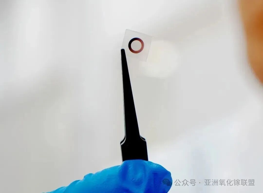
Figure 1. Mg-doped gallium oxide photoconductive switch device
(Source: Shenzhen Pinghu Laboratory)
Core Breakthrough: Comprehensive Upgrade of Mg-Doped Photoconductive Switch
Photoconductive switches are a critical component in high-voltage direct current (HVDC) transmission systems, advanced radar, and pulsed power devices, often referred to as the “lifeline of high voltage systems.” Following its previous milestone in enabling Shenzhen Pinghu Laboratory to achieve a kilovolt-level vertical-structure gallium oxide photoconductive switch, Garen Semiconductor has continued to optimize its doping process and independently produced high-quality Mg-doped gallium oxide materials.
These advances have supported the successful development of the first ten-kilovolt-class gallium oxide photoconductive switch, delivering a qualitative leap in three key performance metrics.
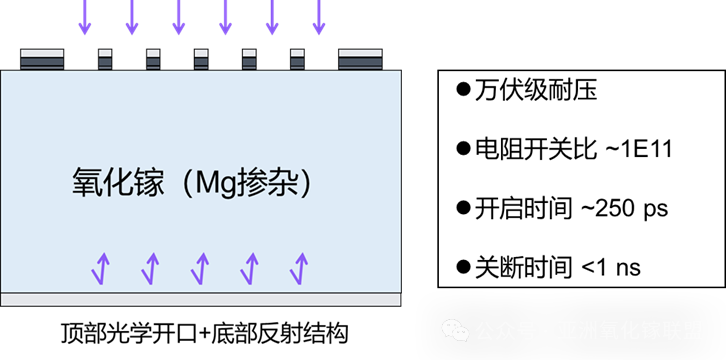
Figure 2. Structure and characteristics of the Mg-doped gallium oxide photoconductive switch
(Source: Shenzhen Pinghu Laboratory)
1. Ultra-High Breakdown Voltage: Withstanding 220 kV/cm Electric Fields
Benefiting from Mg-induced deep-level compensation effects, the device can stably withstand ultra-high electric fields above 220 kV/cm, making it a true “high-voltage workhorse” capable of reliable operation under extreme electrical conditions.
2. Ultra-Low Dark Current: Switching Ratio Reaching 1×10¹¹
Dark current is a key metric for switch performance—higher leakage leads to greater power loss and poorer stability. The Mg-doped device achieves an ultra-low dark current, pushing the switching ratio to the 1×10¹¹ level, about two orders of magnitude higher than mainstream industry levels, effectively addressing the long-standing issue of “leakage in the off-state.”
3. Ultra-Fast Response: Turn-Off Time < 1 ns
Beyond voltage endurance and low loss, switching speed is equally critical. Thanks to the unique advantages of Mg doping, the device achieves a turn-off time of less than 1 ns, combined with a 250 ps turn-on response, enabling ultra-fast switching that is ideally suited for pulsed power systems and advanced radar applications requiring extreme temporal performance.
Technical Foundation: Garen Semiconductor’s Advanced Material Platform
The breakthrough in device performance is fundamentally enabled by the upgrade in substrate and epitaxial material quality. This next-generation Mg-doped gallium oxide photoconductive switch is built upon Garen Semiconductor’s globally leading gallium oxide material technology platform.
As a vertically integrated leader in China’s gallium oxide supply chain, Garen Semiconductor is the world’s first and currently the only company capable of both 8-inch gallium oxide single-crystal substrate mass production and 8-inch homoepitaxial growth, effectively breaking long-standing overseas monopolies in ultra-wide bandgap semiconductor materials.
In March 2025, the company globally launched the 8-inch gallium oxide single-crystal substrate, overcoming key challenges in large-diameter crystal growth. The substrate features excellent crystal quality and extremely low defect density and has already entered mass production and shipment. In March 2026, the company achieved the world’s first 8-inch high-quality homoepitaxial Ga₂O₃ growth, filling a critical gap in large-scale device manufacturing and providing a high-quality foundation for advanced device development.
In addition, Garen Semiconductor is building a fully integrated “equipment–crystal–substrate–epitaxy” industrial chain and has independently developed the “SCIENCE Series” gallium oxide VB (Vertical Bridgman) growth equipment. With full proprietary intellectual property, the system supports multi-orientation and multi-size single-crystal growth, achieving simultaneous advances in material quality and process precision. This ensures 100% self-controlled capability across key segments, providing a solid foundation for large-scale gallium oxide commercialization.
Mission and Commitment: Advancing the Industrialization of Domestic Gallium Oxide
Garen Semiconductor has long been dedicated to the fourth-generation gallium oxide semiconductor field, focusing on the R&D and mass production of high-end substrates and epitaxial materials. Aligning with China’s “15th Five-Year Plan” strategic direction for gallium oxide industrialization, the company emphasizes deep industry–academia–research integration, providing stable and reliable domestic core materials for scientific innovation and device development.
The company also actively participates in industry standard-setting, promoting standardized and high-end development of China’s gallium oxide ecosystem.
Looking ahead, Garen Semiconductor will continue to uphold its commitment to technological innovation, further advancing core R&D and production line upgrades in gallium oxide technologies. The company will accelerate device validation and mass-production integration of 6-inch and 8-inch epitaxial wafers, deepen collaboration across the industrial chain, and empower downstream industries with advanced technologies. These efforts aim to contribute to the high-quality development of China’s semiconductor industry and support the establishment of a global gallium oxide innovation hub.
About GAREN SEMI
Hangzhou Garen Semiconductor Co., Ltd. is a world-leading provider of Gallium Oxide materials and equipment solutions, focusing on R&D and industrialization in the ultra-wide bandgap semiconductor field. The company’s core products include 2–8-inch Gallium Oxide single crystals and substrates (with 8-inch being the world’s first), Gallium Oxide Vertical Bridgman (VB) crystal growth equipment, Gallium Oxide epitaxial wafers, etc. It is committed to building a full-chain product system of “equipment–crystal–substrate–epitaxy” to provide systematic solutions for global customers. The company’s achievements in Gallium Oxide have been specially reported by well-known media including People’s Daily, Xinhua News Agency, Science and Technology Daily, Sina Finance, China Blue News, and The Paper.
Enterprise Honors Summary
Recognized as a National-level Science and Technology Small and Medium-sized Enterprise and Zhejiang Innovative Small and Medium-sized Enterprise in 2023;Awarded Zhejiang Specialized, Sophisticated, Unique and New Small and Medium-sized Enterprise in 2024;Approved as a High-tech Enterprise in 2025;Won the SEMI Outstanding Contribution Award for Sustainable Development at SEMICON CHINA 2025, the Together Progress Award at the Jiufengshan Forum (JFSC) and Compound Semiconductor Industry Expo, the Innovation Vitality Award of Zhejiang Semiconductor Industry, the Second Prize in the Enterprise Group of the 10th “Maker China” Zhejiang Provincial Finals, the Top 500 Enterprise Group of the 10th “Maker China” SME Innovation and Entrepreneurship Competition, and the 2024–2025 Semiconductor Material Industry Contribution Award;The major breakthrough in the preparation of 8-inch Gallium Oxide single crystals and substrates was selected as one of the “Top 10 Advances in China’s Third-Generation Semiconductor Technology 2025” and “Major Scientific and Technological Achievements 2025” by the Department of Science and Technology of Zhejiang Province;Semiconductor Material Technology Innovation Award at the 2026 Hangzhou International Semiconductor and Integrated Circuit Industry Innovation Exhibition;Led the formulation of 2 group standard drafts, participated in drafting 1 national standard, and participated in promoting 1 group standard draft in the Gallium Oxide field;Supported by the “5213” Excellence Program of Xiaoshan District, Hangzhou, Zhejiang Province, and approved to establish Zhejiang Enterprise Research Institute;Obtained the quality management system certification;Granted 20 authorized invention patents at home and abroad (including patents in the US, Japan and other countries), with more than 50 patents pending.
For more information about Garen Semiconductor and its products, please visit our official website: http://garen.cc/
Or contact us via the following ways:
Mr. Jiang: 15918719807
E-mail: jiangjiwei@garen.cc
Mr. Xia: 19011278792
E-mail: xianing@garen.cc
