


News Trends
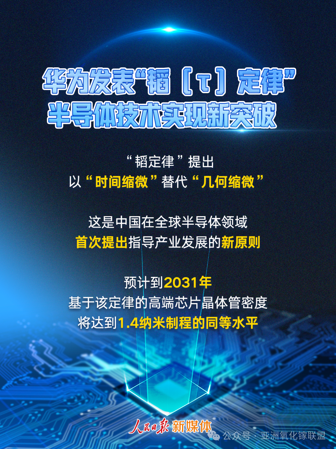
【Domestic News】“Tao (τ) Law”: Huawei Proposes a New Global Principle for the Semiconductor Industry
日期:2026-05-27阅读:134
Huawei Officially Introduces a New Semiconductor Law
Breakthrough in Transistor Density and System Performance Enabled by Logic Folding Technology
At the 2026 IEEE International Symposium on Circuits and Systems (ISCAS 2026) held in Shanghai on the 25th, Huawei Director and Head of the Semiconductor Business, He Tingbo, delivered a keynote speech titled “Exploration and Practice of New Paths in Semiconductors”, in which she officially introduced the “Tao (τ) Law.” This marks the first time China has proposed a guiding principle for global semiconductor industry development. Based on this law, Huawei has successfully designed and mass-produced 381 chips over the past six years. In the coming autumn, Huawei will launch a new Kirin smartphone chip that fully adopts logic folding technology, significantly improving performance.
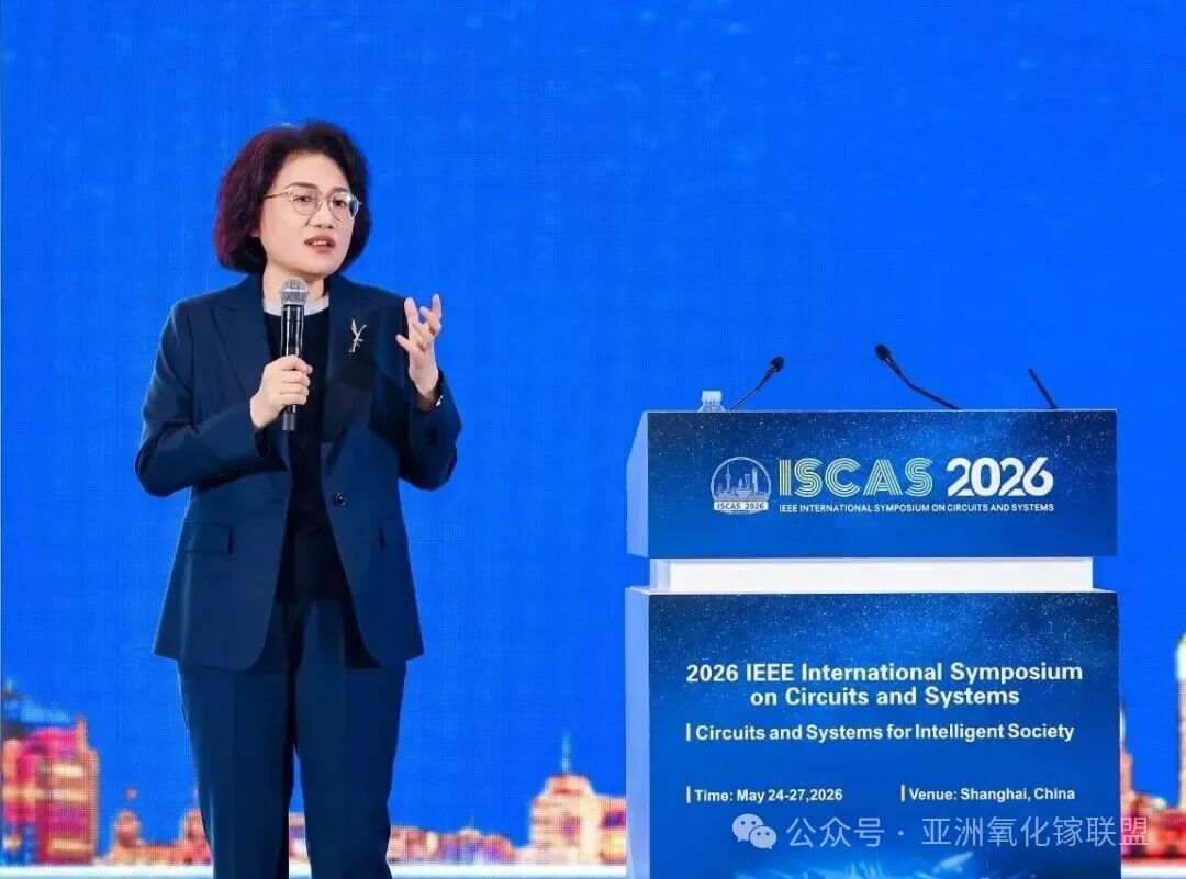
In her keynote speech, He Tingbo formally presented the “Tao (τ) Law.” (Photo by Lin Yuan)
The core idea of the “Tao Law” is to replace the traditional path of “geometric scaling” with “time scaling,” aiming to systematically reduce the time constant (τ) and signal propagation delay, thereby continuously enhancing the overall performance of chips and electronic systems.
For decades, the semiconductor industry has followed Moore’s Law, improving transistor density and chip performance by continuously shrinking transistor sizes. However, as advanced process nodes approach physical and economic limits, the benefits of “geometric scaling” in performance and cost are gradually diminishing. In the post-Moore era, how to sustain computational advancement has become a major challenge for the global semiconductor industry.
Against this backdrop, the “Tao Law” proposes a new technological approach. Rather than relying solely on more advanced process nodes, it emphasizes system-level optimization across devices, circuits, chips, and systems to improve overall efficiency.
A key enabling technology behind the “Tao Law” is “Logic Folding.”
While Moore’s Law relies on continuous transistor scaling (geometric shrinking), modern process technologies are increasingly constrained by physical and cost limits. Huawei’s “Tao Law” shifts the focus from “size” to “time,” targeting the reduction of signal transmission delay (time constant τ) within chips.
Logic folding can be understood as a system-level optimization approach: instead of simply increasing transistor count, it improves overall efficiency through function reuse, path compression, and timing optimization—reducing unnecessary routing and waiting time, and enhancing coordination within the chip. It is not merely about adding more transistors, but about achieving performance gains through architectural and temporal optimization at the system level.
In essence, the “Tao Law” is not a complete replacement for Moore’s Law, but rather a new evolutionary pathway for the post-Moore era, developed under the constraints of approaching physical limits in advanced process technologies.
According to information disclosed at the event, by 2031, high-end chips based on the “Tao Law” are expected to achieve transistor density equivalent to that of 1.4-nanometer process technology.
Regarding the future of the semiconductor industry, He Tingbo stated: “The future belongs to open collaboration. Under the path of the ‘Tao Law,’ we look forward to working closely with global scientists, engineers, and industry partners to jointly advance the continuous development of the semiconductor and electronics industries.”
