


Discover
【Knowledge Discover】A New Era of Ultra-Wide Bandgap Semiconductors: How Gallium Oxide Leads the Fourth-Generation Semiconductor Revolution
日期:2026-05-15阅读:32
Introduction
As next-generation semiconductor materials continue to evolve, gallium oxide is gradually moving from laboratory research into the industrial spotlight. As a representative ultra-wide bandgap semiconductor, gallium oxide demonstrates unique potential in power electronics, ultraviolet detection, and novel optoelectronic devices, owing to its high breakdown field strength, the ability to grow large substrates via melt methods, and solar-blind UV response.
At the same time, gallium oxide still faces numerous challenges before achieving true large-scale industrial application. Every stage—from crystal quality, substrate defects, and epitaxial growth to device architecture, thermal management, reliability, and maturity of the industrial chain—directly impacts its future development boundaries.
Issue 1: Why Is the World So Focused on Gallium Oxide?
From Silicon to Ultra-Wide Bandgap:
The Intrinsic Logic Behind Generational Evolution of Semiconductor Materials
The history of semiconductor materials is a story of humanity’s continuous pursuit of “higher voltage tolerance, higher temperature resistance, and greater efficiency.” Since the 1950s, semiconductor materials have undergone four generational shifts, with each generation establishing an irreplaceable role in specific application areas.
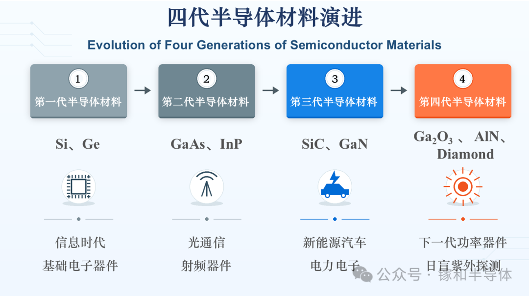
First-generation semiconductors are represented by silicon (Si), with a bandgap of approximately 1.12 eV, forming the cornerstone of the information age. Silicon benefits from highly mature processing technology, low cost, and abundant reserves, and it still dominates the logic integrated circuit field today. However, silicon’s critical breakdown field is only about 0.3 MV/cm, approaching its physical limit in high-voltage (>600 V), high-temperature (>150 °C), and high-frequency scenarios[1].
Second-generation semiconductors are represented by gallium arsenide (GaAs), with a bandgap around 1.4 eV. Thanks to its high electron mobility (~8500 cm²/(V·s)), GaAs has excelled in optical communications (lasers, photodetectors) and RF front-end applications (mobile phone PAs, radar). Yet, its power density is limited, and the toxicity of arsenic restricts its broader adoption in power electronics.
Third-generation semiconductors include silicon carbide (SiC) and gallium nitride (GaN), with bandgaps exceeding 3 eV, earning the designation of wide bandgap (WBG) materials. Tesla Model 3’s main inverter pioneered the use of SiC MOSFETs, increasing driving range by 5–10%; domestic manufacturers such as BYD, NIO, and XPeng are rapidly adopting SiC power modules. GaN, on the other hand, has achieved large-scale commercialization in 5G base station RF power amplifiers and fast-charging applications[2].
Fourth-generation semiconductors, or ultra-wide bandgap (UWBG) materials, feature bandgaps exceeding 4 eV and include gallium oxide (Ga₂O₃, Eg ≈ 4.8 eV), aluminum nitride (AlN, Eg ≈ 6.2 eV), and diamond (Eg ≈ 5.5 eV). Among these, gallium oxide stands out due to the ability to grow single crystals via melt methods, offering a unique cost advantage and attracting intense attention from both academia and industry[3].
Key Takeaways
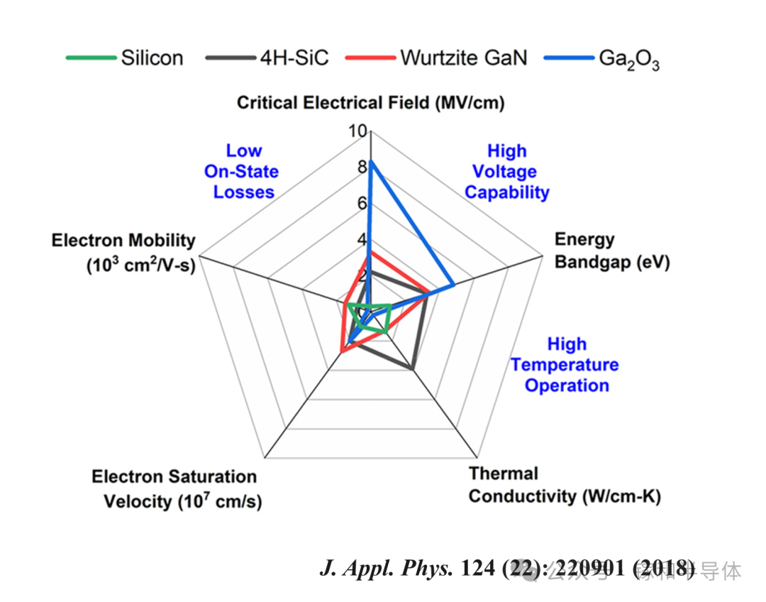
From silicon (Si) to gallium oxide (Ga₂O₃), the bandgap increases from 1.12 eV to 4.8 eV—a 4.3-fold enhancement—while the breakdown field rises from 0.3 MV/cm to 8 MV/cm, representing a 26.7-fold improvement.
This implies that Ga₂O₃ devices theoretically offer higher voltage tolerance and lower intrinsic carrier concentrations, making them well-suited for high-voltage, low-leakage, and high-temperature operation. At the same time, its wide bandgap shifts the intrinsic absorption edge into the deep ultraviolet, giving it a natural material advantage for solar-blind UV detection.
SiC, GaN, and Ga₂O₃ – Differentiated Competition in Next-Generation Power Semiconductors
At the intersection of third- and fourth-generation semiconductors, SiC, GaN, and Ga₂O₃ form a subtle “three-way battle” in the power electronics arena. Each material has its own strengths across parameters such as bandgap, breakdown field, thermal conductivity, electron mobility, and substrate cost, making them suitable for different power semiconductor applications.
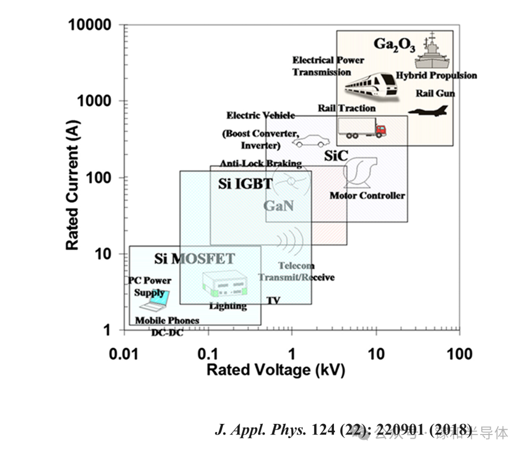
SiC: The Most Mature Wide Bandgap Semiconductor
Silicon carbide (SiC) is currently one of the most industrially mature wide bandgap (WBG) semiconductor materials, especially 4H-SiC. Thanks to its high breakdown field and excellent thermal conductivity, it has become a core material in electric vehicles, power electronics, and high-voltage power modules. Substrate technology is advancing from 6-inch to 8-inch wafers, and companies such as Wolfspeed, ROHM, and STMicroelectronics have established relatively mature automotive-grade SiC MOSFET production lines.
However, the high performance of SiC comes with a high substrate manufacturing cost. Bulk single-crystal growth mainly relies on high-temperature physical vapor transport (PVT)/sublimation methods, which require elevated temperatures, slow growth rates, and challenging defect control and crystal processing. As a result, SiC substrates remain significantly more expensive than silicon-based materials[4].
GaN: The King of High-Frequency Applications
Gallium nitride (GaN) excels in “speed.” Its electron mobility is around 1,200 cm²/(V·s) and saturation drift velocity reaches approximately 2.5 × 10⁷ cm/s, both surpassing SiC, making it particularly suitable for high-frequency switching, fast-charging power supplies, and RF power applications. Leveraging the two-dimensional electron gas channel formed in AlGaN/GaN heterostructures, GaN HEMTs achieve low on-resistance and high-speed switching. Companies such as Navitas, Innoscience, and Infineon/GaN Systems have promoted large-scale applications of GaN fast-charging chips.
However, GaN also has notable limitations: large-size, low-cost homoepitaxial substrates are still immature, and commercial power devices mainly rely on GaN-on-Si or GaN-on-SiC heteroepitaxy. Defects and stress caused by lattice and thermal mismatch, along with leakage and trap effects in the buffer layer, present significant challenges for vertical high-voltage power devices[5].
Ga₂O₃: A Cost-Competitive Challenger Rising from Behind
At the level of intrinsic material properties, β-Ga₂O₃ features an ultra-wide bandgap of approximately 4.8 eV and a theoretical breakdown field of about 8 MV/cm, both surpassing SiC and GaN. However, Ga₂O₃’s most differentiated advantage in industrialization is not limited to its material parameters—it lies in its ability to grow bulk single crystals using melt-based methods such as Czochralski, Edge-Defined Film-Fed Growth (EFG), and Bridgman/Vertical Bridgman techniques. Unlike SiC, which mainly relies on high-temperature PVT/sublimation methods, the melt growth of Ga₂O₃ occurs at around 1800 °C, lower than the >2200 °C typically required for SiC PVT growth. Melt-based growth also offers higher efficiency and better scalability for large-diameter crystals. In theory, this enables Ga₂O₃ substrates to achieve significantly lower costs than SiC in large-scale manufacturing. If challenges such as low thermal conductivity, difficulty in p-type doping, epitaxial defects, and device reliability can be addressed, Ga₂O₃ is poised to establish differentiated competitiveness in cost-sensitive medium- to high-voltage power devices and solar-blind ultraviolet detection applications.
Key Differences
Overall, SiC, GaN, and Ga₂O₃ are not simply interchangeable materials; rather, they compete in a differentiated manner across distinct application scenarios. Ga₂O₃ stands out for its wider bandgap, higher theoretical breakdown field, and the potential for low-cost, large-size single-crystal substrates grown via the melt method. If future breakthroughs address challenges in thermal management, epitaxial defects, and device reliability, Ga₂O₃ could unlock new applications in medium- to high-voltage, cost-effective power devices as well as solar-blind ultraviolet (UV) detection.
From Lab to Industry: The Strategic Value and Global Landscape of Gallium Oxide
Cost Revolution: Breaking the High-Price Material Barrier
In the cost structure of power devices, the substrate is a key factor affecting the final device price. SiC substrates have long been expensive, limiting their scalability and broader, cost-effective adoption. Ga₂O₃’s key differentiation lies in its ability to grow single-crystal substrates via the melt method, a process more akin to sapphire and other oxide crystals, theoretically offering significantly lower costs than SiC. As large-size (6-inch) Ga₂O₃ substrates and epitaxial wafer technologies gradually mature, this cost advantage is expected to expand further, providing a more economically viable materials pathway for medium- to high-voltage power semiconductors.
Application Scenarios: The Natural Domain of Ultra-High Voltage
The core advantages of Ga₂O₃ stem from its ultra-wide bandgap and extremely high theoretical breakdown field. For applications such as power grids, renewable energy conversion systems, high-voltage power supplies, rail transit, and aerospace power systems, Ga₂O₃ offers the potential for reduced theoretical on-resistance through thinner drift layers and higher doping concentrations. However, actual device performance is still strongly dependent on epitaxial quality, thermal management, edge termination design, and long-term reliability.
In addition, its 4.8 eV bandgap corresponds to an absorption edge of approximately 258 nm, located within the solar-blind ultraviolet region. This endows Ga₂O₃ with inherent material advantages for applications such as flame detection, corona discharge monitoring, space-based UV sensing, secure communication, and specialized detection systems.
International Strategy: Global Deployment Trends
Globally, Japan has been one of the earliest countries to advance Ga₂O₃ industrialization. Leveraging long-term technological accumulation at NCT, Tamura, NICT, and Tokyo University of Agriculture and Technology, Japan has become a key supplier of β-Ga₂O₃ substrates and homoepitaxial wafers.
In the United States, institutions such as AFRL have focused on Ga₂O₃ high-voltage power devices at an early stage, conducting systematic studies on MOSFETs, FinFETs, breakdown characteristics, and device reliability. These efforts have helped transition Ga₂O₃ from a material-level advantage to practical device structure validation.
China has also been rapidly catching up in recent years, with research institutes, universities, and enterprises actively pursuing crystal growth, epitaxial fabrication, defect control, device design, and process integration. Ga₂O₃ is gradually moving from isolated research efforts toward a new stage of coordinated development across materials, epitaxy, and device technologies.
Summary of This Issue
Gallium oxide is no longer just a “concept material” confined to the laboratory—it is emerging as an ultra-wide bandgap semiconductor moving toward industrial validation. Its combination of a wider bandgap, higher theoretical breakdown field, and the potential cost advantages offered by melt-grown single-crystal substrates establishes its core competitiveness, setting it apart from SiC and GaN.
Of course, Ga₂O₃ is not without limitations. Lower thermal conductivity, relatively limited electron mobility, challenges in p-type doping, and device reliability remain key obstacles to large-scale application. Nevertheless, Ga₂O₃’s development logic is not about simply replacing SiC or GaN; rather, it aims to create differentiated advantages in mid-to-high voltage, cost-effective power devices, and solar-blind ultraviolet detection.
Overall, understanding the material positioning of Ga₂O₃ not only helps clarify the evolution of fourth-generation semiconductors but also provides insight into the future trajectory of power electronics and deep-UV optoelectronic devices.
[1] B. J. Baliga, Journal of Applied Physics, 1982, 53, 1759.
[2] T. Kimoto, J. A. Cooper, Wiley-IEEE Press, 2014.
[3] S. J. Pearton, J. Yang, P. H. Cary, F. Ren, J. Kim, M. J. Tadjer, M. A. Mastro, Applied Physics Reviews, 2018, 5, 011301.
[4] D. Nakamura, I. Gunjishima, S. Yamaguchi, T. Ito, A. Okamoto, H. Kondo, S. Onda, K. Takatori, Nature, 2004, 430, 1009-1012.
[5] U. K. Mishra, Shen Likun, T. E. Kazior, Yi-Feng Wu, Proceedings of the IEEE, 2008, 96(2), 287-305.
[6] A. Kuramata, K. Koshi, S. Watanabe, Y. Yamaoka, T. Masui, S. Yamakoshi, Jpn. J. Appl. Phys, 2016, 55, 1202A2.
[7] R. Suzuki, S. Nakagomi, Y. Kokubun, Applied Physics Letters, 2011, 98, 131114.
[8] M. Higashiwaki, K. Sasaki, A. Kuramata, T. Masui, S. Yamakoshi, Applied Physics Letters, 2012, 100, 013504.
[9] S. J. Pearton, Fan Ren, Marko Tadjer, Jihyun Kim, J. Appl. Phys, 2018, 124 (22): 220901.
